PG31 GPS USB Dev Board
Description:
You've probably heard about the CP210x USB ICs from Silicon Labs, now here's an application that uses it. The CP2102 gives us 3V TTL to a VCP (virtual comm port) over USB as well as generating the 3.3V needed for the board.
In this project we demonstrate how to:
- Setup a USB to Serial link
- Use the CP2102 for 3.3V
- Use a SMD 12mm battery holder
Contents
USB Connection
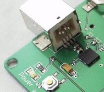
The CP2102 USB IC is fairly easy to use once you've plugged it down a couple times.
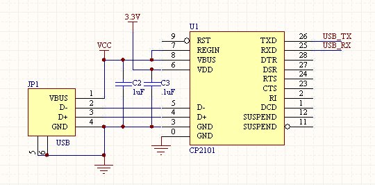
The USB connector has four pins : Vcc (*around* 5V), GND, D+, D-. Tying these four connections to the CP2102 is easy enough.
There are a couple things to note. In this setup, we do not have any ESD protection or surge supression. We are quite possibly violating some USB standards. But does it work? Yep.
When you configure the CP2102 this way, it can source up to 100mA at 3.3V using its internal voltage regulator. This is perfect for our application as the PG31 needs ~40mA at 3.3V.
Note the TX pin on the CP2102 is an output and needs to be connected to the RX pin on the PG31. This screwed me up a few times.
The CP2102 has built-in cystal and eeprom. These means you need very few external components to get it working. You can even program in your own ID string so when you plug it onto your computer, it comes up with the name of your widget!
When the CP210x is attached to a computer (and it's soldered correctly) you will see windows hardware wizard request drivers. These drivers can be downloaded from SI Labs. You can also create your own signature drivers using some SI Labs software.
You can also program the internal EEPROM to reflect your own product ID and serial strings. This software is from SI Labs as well but I forget were - when someone finds it, post it here.
Once the drivers are installed, the CP210x will turn into a serial com port! Yes! It's weird to think about until you see it happen. So this USB dev board now acts like a com port on my computer. All I have to do is pass characters in and out COM 5 (for example) and I can do things over USB! No messy drivers, no protocols to think about, it's all done in the IC. All right!
One thing to note when you are using the CP210x ICs, the Linux community may scoff. SI Labs did a great job with the windows support, but a piss-poor job of opening the drivers for the open-source community. I'm not really a Linux person so it didn't effect me. But if your app needs linux connectivity, you may want to take a quick look for other potential ICs. Last I heard, there was good Linux support for the CP2102, but there was nothing for the CP2103 GPIO control...
One last con : The ICs come in QFN leadless package only. YES it can be soldered by hand, but you'll need some experience and/or some good hot-air soldering tools. I taught myself how to rework stuff using this IC. You really can't destroy it, but you can certainly delaminate (kill) the PCB if you heat it for excessive amounts of time. Don't 'not' create a PCB or a design because of silly SMD parts. They're not that hard to solder!
Battery Backup
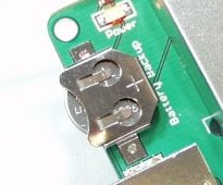
If you're playing with GPS, you've got to have a battery backup. The 12mm coin cell lithium allows the PG31 (and many other GPS receivers) to retain the alamanac data. This small battery provides just enough juice for 3-5 years. By having alamanac data at power on, the GPS receiver will be able to do a warm lock instead of a cold lock. Cold locks take 1-2 minutes, warm locks, as little as 30 seconds. The alamanac data, in effect, allows the GPS receiver to 'guess' where it is in the world ("Last time I was on I was in Ohio, therefor, I will assume I'm near there").
If you're unfamiliar with Lithium Coin Cells - they come in a couple different sizes. I prefer 12mm just cause it's small but beefy enough to do most of the BBR (battery backed ram) that we need to support. The battery itself has a postive top (noted by the plus) and a ground on the bottom. You normally create a pad on the PCB for the ground and the coin cell holder is positive. We've learned the hard way that the bottom part of the cell is sometimes concave. This means that when you slide the coin cell onto the board, the concave ground part of the cell may not contact the PCB pad very well. If you're using a paste stencil, just leave a cutout for this pad. The extra paste will add 5-10 mils of solder to the pad. If you're solder the thing by hand, add a little blob of solder to this ground pad to give it some height. When you insert the battery, it should ride nicely on top of the ground pad blob.
PG31 Footprint
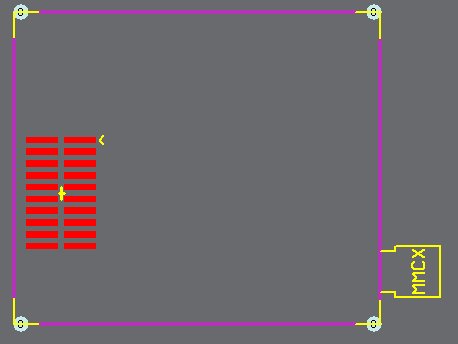
Now about the footprint for the PG31. Unless the manufacturer hands you a foorprint file or a simple, recommended FP in the datasheet, you're going to have to go it on your own. We took the PG31 and a pair of calipers and went at it. It can be extremely difficult the first time. This PG31 FP took me twice to get correct. Do the best you can and try to account for things like the antenna connector. The second rev FP, I forgot to account for the MMCX connector, I put the DB9 connector right up against the PG31, and Viola - useless PCB! a.k.a another coaster for my coffee cup. But once you've got the FP, you're good for all future projects using that device. Now you know when engs hate to change parts...
Final Layout
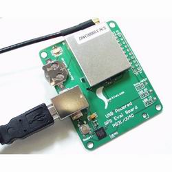
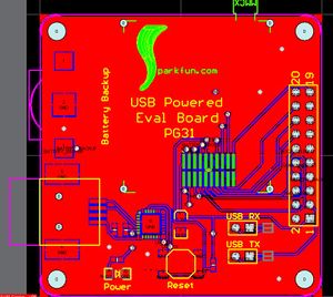
You can see the PCB layout is pretty straight forward. The 'solder jumpers' are a feature that SFE came up with to minimize our manufacturing time while allowing end users to populate the physical jumpers if they needed the ability to connect/disconnect a feature often and quickly. Most users just plug the PG31 onto their computer for quick evaluation. At some point, the CP2102 IC may need to be disconnected from the circuit so that an external micro or embedded system could be attached. If this is done back and forth often, the end user can clear the solder jumper with a swipe of the soldering iron, install a 2-pin header and a black plastic jumper. This now allows them to jumper/dejumper quickly and keeps us from having to solder the 2-pin headers into a board that may not need them.
Things to Improve
So that's pretty much it. The board works well, and assuming Laipac doesn't change their parts again, we will produce the board for some time.
We may consider migrating to a different USB IC someday but the CP2102 continues to be a really simple to use USB to UART IC.
Documents
Footprints:
SFE Footprint Library
FP Name: PG31
Supplier Info:
Spark Fun Electronics part # : Eval-PG31-USB
Single Piece Price : $29.95
Related Items:
