Difference between revisions of "Programmable Chip EEG"
(revert to Josh eeg 14:06, 9 December 2006) |
|||
| Line 29: | Line 29: | ||
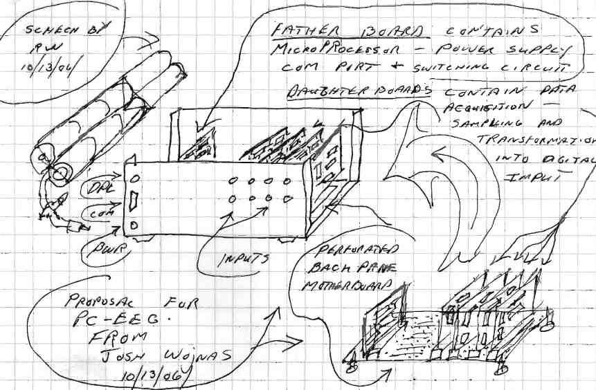
Here is a diagram of how the analog signal processing boards and the microprocessor board will come together. | Here is a diagram of how the analog signal processing boards and the microprocessor board will come together. | ||
[[Image:Pceeg.jpg]] | [[Image:Pceeg.jpg]] | ||
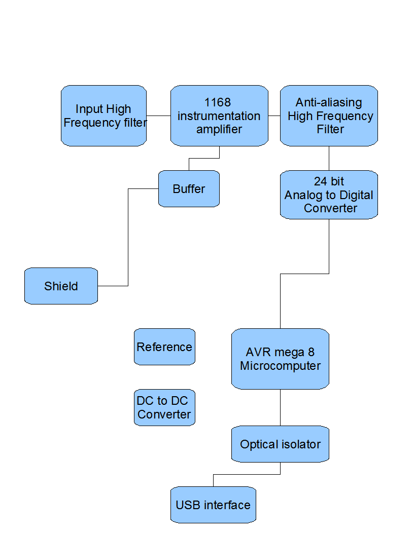
| + | Here is how the analog signal prossesing board will come together. | ||
| + | [[Image:newpceeghddesign.png]] | ||
== Description of How it Works == | == Description of How it Works == | ||
Revision as of 22:53, 22 December 2006
Contents
The Programmable Chip EEG
Welcome to the PCEEG Wiki, where everyone can add to this EEG brain-computer interface!
PCEEG, What it is and why it can be the best
- The The Programmable Chip EEG gets its name because its hardware and software can be adjusted digitaly from a home pc.
- The hardware can be adjusted by Digitally Programmable Potentiometers. They are used to set the Gain, and frequency responce.
This is usefull to calibrate multiple analog boards for different EEG tests.
- The Programmable Chip EEG is a Modular Multi-channel electroencephalograph.
- This can be used for a brain-computer interface with biofeedback using a flex sensor or servo to detect fingure movements.
- The LT1168 Programmable-Gain Precision Instrumentation Amplifier is used to amplify the weak electric signals coming from the brain through electrodes attached to the scalp, and has internal protection circuitry for the user.
- Several matched LT1114 Low Power Precision OP-Amps are used for amplification and filtering of the signals.
- The Digitally Programmable Potentiometers AD5204 4-Channel Digitally Controlled Potentiometer is used to make calibration of this device easier. (Historically, a weak point of homebrew designs has been their sensitivity to component value; tolerance and drift have made them require constant tweaking for good results.)
- To reduce noise in the readout of the analog part of this circuit, a common-mode feedback is passed back into the body by the driver right leg circuit. Band reject filter may also be used (to reject, for example, 60Hz noise from nearby A/C power wiring).
- The analog signal prossesing board will digitise the signal and pass the data to the control board. The control board is based on the AVR Butterfly which will, further process the signals, and provide an interface to a computer & lcd display.
Status
We currently have a (preliminary?) circuit design and a (prelimary) PCB layout. We are using LT switcher CAD to draw the scematic.
Hardware Overview
Here is a diagram of how the analog signal processing boards and the microprocessor board will come together.
 Here is how the analog signal prossesing board will come together.

Description of How it Works
The daughter signal prossesing board is responcible for filtering and digitising the signals from the body, then the signals are passed to the control board that is the motherboard. The motherboard then can pass the signal to a larger computer.
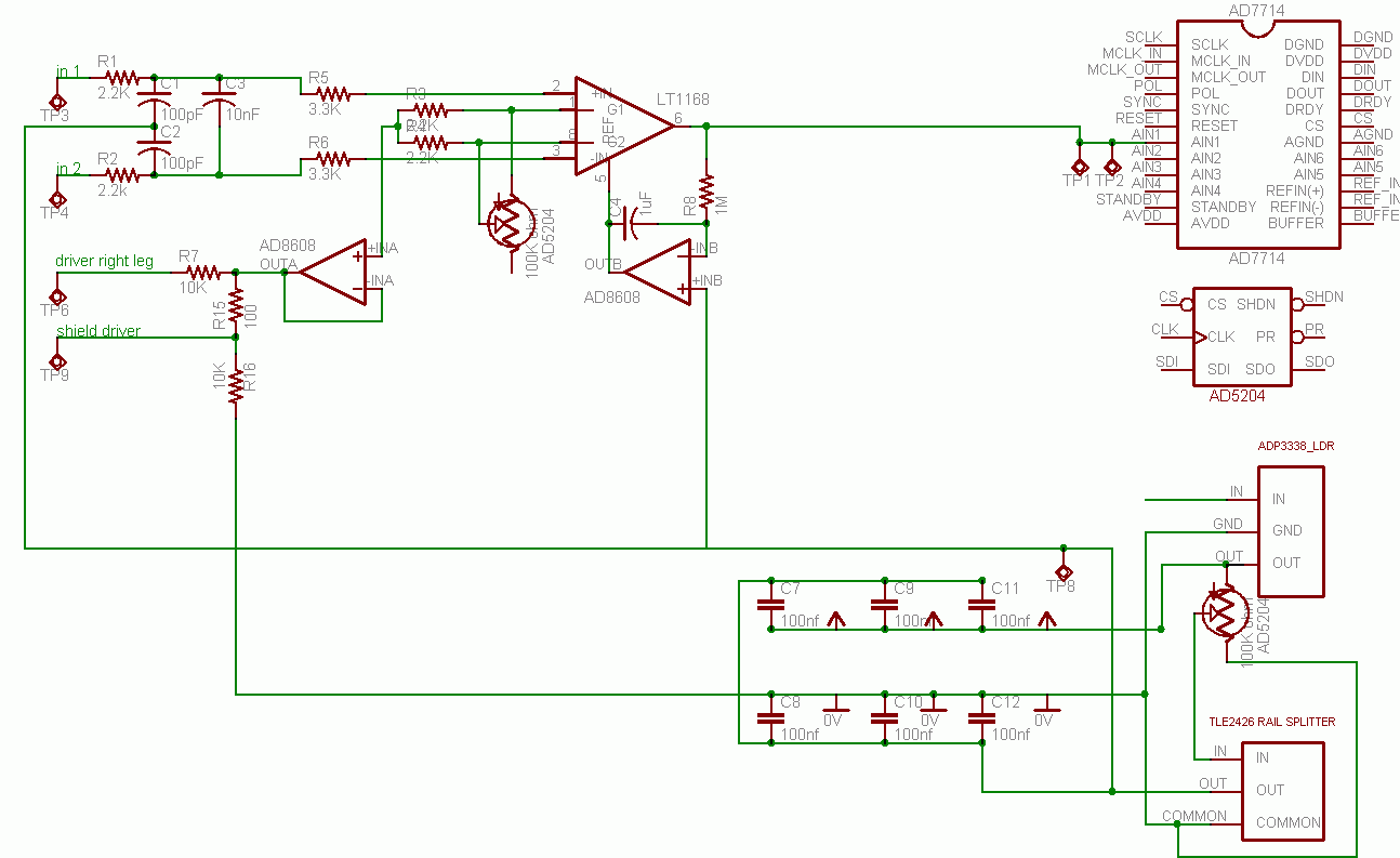
The differential analog signal is amplified by the instramentation amplifier. Then the signal is amplified and conditioned by high pass and low pass filters.
The common mode signal is inverted summed and sent back to the body to decrese common mode signal thsi is done by the driver right leg circuit.
Band reject filters may be added soon in the future.
Then the analog signals are simultaniously digitized and the digital values can be clocked to the controler motherboard.
The controler board that is the mother board of the system and the signal prossesing daughter boards plug into is the AVR Butterfly
How You Can Help
- . get the tools
Software Tools
- We are using LT switcher CAD to draw the scematic. This also is a SPICE Simulator used to analize the amplifier design.
- Eagle CAD could be used in the future after all the parts are surface mount & the analog sections are alalised. To autorout future designs.
- Express PCB is being used to create the first PCB but surface mount must be used to save hole count and space.
- Maxima a computer algebra system s used for graphing and matth displays.
- I2C interface diagram for programmable resistors and a/d converters 12 or more bits with low cost.
- SPI interface diagram for programmable resistors and a/d converters 12 or more bits with low cost.
- linear switcher cad schematic drawing from PCEEG technology applied to the Open EEG design with improvements.
- migrate from switcher cad to pcb express.
- migrate from pcb express to eagle cad after testing to further development.
Parts used in the PCEEG:
- LT1168 Programmable-Gain Precision Instrumentation Amplifier is used to amplify the weak electric signals coming from the brain through electrodes attached to the scalp, etc.
- Several LT1114 Low Power Precision OP-Amps are used for amplification and filtering of the signal
- The Digitally Programmable Potentiometers AD5204 4-Channel Digitally Controlled Potentiometer is used to make calibration of this device easier. (Historically, a weak point of homebrew designs has been their sensitivity to component value; tolerance and drift have made them require constant tweaking for good results.)
To reduce noise in the readout of the analog part of this circuit, a common-mode feedback is passed back into the body by the driver right leg circuit. Band reject filter may also be used (to reject, for example, 60Hz noise from nearby A/C power wiring).
The analog signal prossesing board will digitise the signal and pass the data to the control board. The control board is based on the AVR Butterfly which will, further process the signals, and provide an interface to a computer & lcd display.
News
The design is switching to EAGLE CAD, because the auto-router is excellent for open-source productivity. It will allow the design to evolve faster and with less work with a wider selection of PCB Manufacturers.
Here is a picture of the PCEEG being done in EagleCAD.

The ideas and monkey to robot arm interface by Miguel Nicolelisis very inspiring. He used implanted electrodes to monitor and allow monkeys to control a robot arm as if it was their own. Could the PCEEG do the same with its electrodes on the scalp. Only the future will show.
Open Source Circuit Design
Open source (public) results!
PHP will be used to create a database of users and what they sample and choose to share with the open source community.
The database will give statistical analysis on users recordings.
Also the extension of SETI called BIONIC could be used as a distributed library creation of artifacts and data mining.
Please contribute and make the PCEEG a great tool for researching brain computer interfaces.
A/D Converters
The programmable chip EEG needs an A/D converter to convert the analog signal (at the output of the instrumentation amplifier) into digital bits. We expect this project to require at least 12 bit ADC.
Many Atmel and other microcontrollers have a built-in ADC, but those are at most 10 bit ADC, so that ADC is useless to us -- we are forced to use an external ADC.
What low-cost ADC are available with at least 12 bits?
- $2.50 MCP3301 has 1 ADC input (13 bits)
- $3.50 MCP3302 has 2 ADC input (13 bits)
- $3.50 MCP3204 has 4 ADC input (12 bits)
- $4 MCP3208 has 8 ADC input (12 bits)
- $8 dsPIC30F 2011 microcontroller has 8 ADC inputs (12 bits). See dsPIC30F 5011 Development Board for details.
- $6 CY8C27443 Cypress PSoC microcontroller has 4 ADC inputs (14 bits) -- but what is the sampling rate? Also has 4 DAC outputs (9 bits).
- biosemi used analog devices AD7716 22 bit
The newest system is a dc amplifier without a high-pass, and all the low-pass filtering is digital
The Goal
Eventually, kits could be sold, if there were interest. More info is available at the PCEEG SourceForge home page at PCEEG sourceforge.net.