Difference between revisions of "Basic Circuit Building Blocks"
Russ hensel (talk | contribs) |
|||
| (204 intermediate revisions by 47 users not shown) | |||
| Line 1: | Line 1: | ||
| − | These are circuits and parts of circuits that we see over and over again in larger projects. Understanding a complex circuit is much easier if you understand these building blocks. | + | These are circuits and parts of circuits that we see over and over again in larger projects. Understanding a complex circuit is much easier if you understand these building blocks. |
| − | == | + | Operational amplifier are the basis for many circuit building blocks especially in the range of DC to 1 meg Hz. See [[OpAmp Links]]. |
| + | |||
| + | == Introduction and Page Status.... == | ||
| + | ( Some of schematics have been drawn in Eagle and the screen captured, use other methods if you wish. Feel free to add your own circuits, as long as they are basic building blocks, there are lots of other places for project circuits. If you get into more advanced circuits, give them their own page and link to them. Some entries are not complete, if the explanation of the circuit does not match the diagram that is a good tip off. ) | ||
| + | <br> | ||
| + | To Do | ||
| + | * Why not put alpha order? | ||
| + | * work on external links | ||
| + | |||
| + | More circuits that would be good to add | ||
| + | |||
| + | *AC Coupling Capacitor / High Pass Filter | ||
| + | *Battery Lamp and Switch | ||
| + | *Diode Rectifier | ||
| + | |||
| + | [http://forum.allaboutcircuits.com/showthread.php?t=32697 Current rating and full wave rectification] | ||
| + | *LM35 Temperature Sensor | ||
| + | *555 Timer astable oscillator | ||
| + | *[[current mirror]] | ||
| + | **Transistor Current Mirror | ||
| + | *charge pump | ||
| + | *diode for forward drop bias voltage | ||
| + | *diode logical or | ||
| + | *H Bridge | ||
| + | |||
| + | An H bridge is an electronic circuit that causes current to flow in one direction or the other ( from a single ended power supply ). Often used for motor control [[motor driver]]. | ||
| + | It is an electronic double pole double throw switch. | ||
| + | **[http://code.rancidbacon.com/Electronics] See Section on ''H-Bridge'' | ||
| + | **[http://roko.ca/robotics/h-bridge-fundamentals H-Bridge Fundamentals] | ||
| + | *integrator | ||
| + | *diode full wave bridge | ||
| + | *RC timer | ||
| + | *RF Mixers | ||
| + | *diode rounding circuit | ||
| + | *row and collumn connection | ||
| + | *sample and hold http://en.wikipedia.org/wiki/Sample_and_hold | ||
| + | *Simple Oscillator circuits | ||
| + | *transformer | ||
| + | *voltage multiplier and voltage doubler | ||
| + | |||
| + | |||
| + | *[[Colpitts Oscillator]] | ||
| + | |||
| + | Links to basic circuits: | ||
| + | |||
| + | *[http://electricalengineeringforbeginners.blogspot.com/ Donny's Learn Electrical Engineering for Beginners] | ||
| + | *[http://webpages.ursinus.edu/lriley/ref/circuits/circuits.html DC/AC Circuit Reference] | ||
| + | *[http://www.educypedia.be/electronics/analogdiode.htm Educypedia] A web site of links. Lots of material. | ||
| + | |||
| + | <!---------------------------------------------------------------------> | ||
| + | |||
| + | == Amplifiers == | ||
| + | An amplifier is any circuit which has a larger output than input, typically either larger voltage or larger current, or both. Generally larger power out than in. Several of the circuits here are amplifiers, but as these are only basic circuit, many types of amplifiers are omitted here. | ||
| + | |||
| + | See the sections on: Op amp Non Inverting Amplifier, Op amp Unity Gain Buffer .... | ||
| + | |||
| + | *[http://www.amplifiersite.com/ AmplifierSite.com] | ||
| + | *[http://electronicdesign.com/Portals/0/TI_Wp_AudioGuide_Aug2011.pdf Guide to a lot of amplifier and other audio circuits] | ||
| + | |||
| + | == Current Sense Resistor ( Shunt Resistance ) == | ||
| + | |||
| + | A current Sense Resistor is a low value of resistor that is placed in series with some other circuit. We can then measure the voltage across the resistor to compute the current. If the resistor has a low value compared to other components we can ignore the effect on the circuit. We use the word shunt when the voltage is measured by a device that has a fairly low resistance itself. We then have to do a more careful calculation of how the current is shared by the two devices. | ||
| + | |||
| + | Circuit: | ||
| + | [[Image:shunt.png | Shunt Resistance ]] | ||
| + | |||
| + | Where | ||
| + | *R shunt resistor used to sense the current ( and divert it from the meter ). Usually much less in value than the internal resistance of the meter. | ||
| + | *METER meter or other device used to measure the voltage across the shunt resitor. Often the resistance of the meter is ignored ( if high ). | ||
| + | *BATTERY a battery or other voltage source. | ||
| + | *BULB an incandescent light bulb | ||
| + | |||
| + | Discussion: | ||
| + | |||
| + | In the old days a sensitive meter, say 50 mv full scale, would be used with a set of shunt, some looking like metal bars, to measure a wide range of currents, up to and exceeding 50 amps. Sometimes a meter came with a set of shunts for measuring different currents. See links. A completely different way to measure currents is to use a hall effect sensor. | ||
| + | |||
| + | |||
| + | Links to More information: | ||
| + | #[http://www.scienceshareware.com/bg-current-monitoring.htm Scienceshareware.com's How A Precision Resistor Is Used to Measure / Calculate Current and Power in an Electrical Circuit.] | ||
| + | #[http://www.maxim-ic.com/appnotes.cfm/appnote_number/746/ High-Side Current-Sense Measurement: Circuits and Principles] | ||
| + | #[http://en.wikipedia.org/wiki/Shunt_(electrical) Shunt (electrical) From Wikipedia, the free encyclopedia] | ||
| + | * Other ways to measure current: [[Motor_driver#current_sense]] | ||
| + | |||
| + | == Current Limit or Constant Current ( Transistor Based ) == | ||
| + | |||
| + | This is a modification of the emitter follower to limit the current output. So if your output stage is an emitter follower you can add current limiting to it. Or given enough input drive, say from a voltage divider it will act as a constant current source. | ||
| + | |||
| + | Circuit: | ||
| + | [[Image:cc_limit.png |thumb|450px| Current Limit or Constant Current ]] | ||
| + | |||
| + | Where | ||
| + | *R1 base resistor to limit base current to transistor Q1. | ||
| + | *R2 current sense resistor used to sense the current and turn on transistor Q2. | ||
| + | *Q1 main transistor supplying the load current. | ||
| + | *Q2 current limiting transistor. | ||
| + | |||
| + | Discussion: | ||
| + | |||
| + | The idea here is that R2 is a current sense resistor. When the sense voltage across R2 reaches about .7 ( for silicon transistors ) Q2 begins to conduct and diverts the base drive from Q1 cutting its output current. So the max. current from the circuit is reached when I*R2 = .7. This circuit can be used to protect amplifiers ( including push pull amps. ), power supplies and other circuits; or it can be used as a constant current circuit. It is not a precision circuit, but it is cheap, simple, and effective circuit. | ||
| + | |||
| + | |||
| + | More information: | ||
| + | #[http://freecircuitdiagram.com/2008/08/27/variable-adjustable-current-limiter-circuit/ Variable (Adjustable) Current Limiter Circuit ] This is a bit more complicated version using a transistor to drive a darlington transistor, with the limit being adjustable. | ||
| + | #[http://forum.allaboutcircuits.com/showthread.php?t=32709 Current Source for Resistance Measurement] | ||
| + | #[http://powerampdesign.net/images/AN-12_The_Problem_with_Current_Limit.pdf The Problem with Current Limit] Discusses this circuit as applied to a power amplifier. | ||
| + | #[http://www.instructables.com/id/Constant-current-LED-Tester/ Constant current LED-Tester] Simple application of the circuit as an LED tester. | ||
| + | |||
| + | == Filter Capacitor / Decoupling Capacitor / Low Pass Filter == | ||
| + | Circuit: | ||
| + | [[Image:filtercap.png | Filter Capacitor ]] | ||
| + | |||
| + | Where | ||
| + | *D2 is a diode, it lets current pass only in the direction of the arrow. | ||
| + | *R resistor | ||
| + | *Input a source of alternating current ( occasionally DC in which case the whole circuit serves only to protect against a reverse connection. | ||
| + | C1 the first, main, filter capacitor. | ||
| + | C2 the second filter capacitor. | ||
| + | |||
| + | Discussion: | ||
| + | In this circuit C1 is a classic filter capacitor it charges while the diode conducts, it discharges and supplies current when the diode does not. R and C2 are a second stage filter. With R set to 0, it simply adds to the value of C1. With R in the circuit it forms a low pass filter which helps remove the ripple from the power ( at the cost of some voltage drop ). In the old days R would often be a low value inductor which had a similar effect without the voltage drop. A capacitor alone is often put across a circuit component that uses power to supply bursts of current and stop noise from being propagated through the power supply. | ||
| + | |||
| + | The amount of ripple in a simple circuit like this can be determined from the supply frequency voltage, output current, and the capacitance. The amount of time without any input voltage is 1/2f. Given an output current I, the charge transferred is is I/2f. The voltage sag is then just the charge divided by the capacitance, or I/2fC. An inductor added to this circuit will compensate for voltage sag by inducing a voltage if the current starts to drop. | ||
| + | |||
| + | <!----------More Information: | ||
| + | <!---------------------------------------------------------------------> | ||
| + | |||
| + | == High Side Switch == | ||
| + | |||
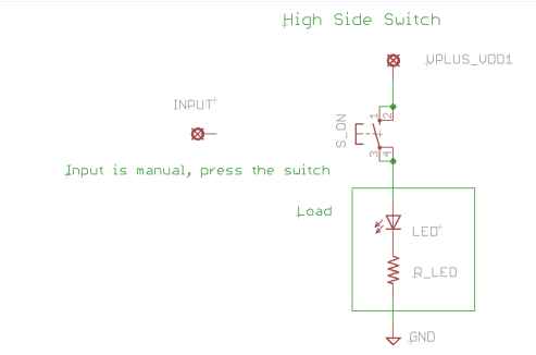
| + | This circuit switches a load at the high side away from ground. With a simple switch it is easy, just wire the switch into the high side. Using transistors is not so easy. There are integrated circuits that make it easy again. But this is not a basic circuit. Contrast with [http://opencircuits.com/Basic_Circuits_and_Circuit_Building_Blocks#Transistor_Low_Side_Switch Transistor Low Side Switch] | ||
| + | |||
| + | == Light Emitting Diode ( with current limiting resistor ) == | ||
| + | |||
| + | Use this circuit to light low power LEDs | ||
| + | |||
| + | A light emitting diode can be very sensitive to small voltage changes, just a bit too much voltage and the LED will draw too much current and “burn out”. Thus it is often used with a resistor in series. If we have a 5 volt source of voltage and an LED that is specified for 2.5 volts at 10 ma, then the resistor must have ( 5 – 2.5 ) volts = 2.5 volts and 10 ma. Using ohms law 2.5/10 x 10 ee-3 = 250 ohms. | ||
| + | |||
| + | A transistor low or high side switch can be used with the resistor if your input cannot supply enough current for the LED. | ||
| + | |||
| + | Circuit: | ||
| + | [[Image:ledres.jpg | LED and current limiting resistor ]] | ||
| + | |||
| + | Where | ||
| + | *LED the LED | ||
| + | *R_LED the current limiting resistor | ||
| + | *INPUT voltage source for lighting the LED | ||
| + | |||
| + | More information: | ||
| + | *[http://www.seattlerobotics.org/encoder/mar97/basics.html Very Basic Circuits ] | ||
| + | *[http://www.iguanalabs.com/1stled.htm Learning About Transistors and LEDs ] | ||
| + | *[http://quantsuff.com/index.htm WELCOME TO QUANTSUFF'S CIRCUIT PAGE. Low Voltage, high-efficiency Drivers for LED Lights ] | ||
| + | *[http://www.dnatechindia.com/index.php/Tutorials/8051-Tutorial/LED-Interfacing.html Interfacing LED to 8051 Microcontroller] | ||
| + | *[http://www.evilmadscientist.com/article.php/throw Some thoughts on throwies] interesting notes on the resistor normally used with an LED. | ||
| + | |||
| + | == Op Amp Non Inverting Amplifier == | ||
| + | Use this circuit where the signal you have is not as large as you want, or cannot provide enough current. It is called non inverting because a positive input produces a positive output ( An inverting amplifier produces a negative output when given a positive input ). | ||
| − | |||
Circuit: | Circuit: | ||
| − | [[Image: | + | [[Image:opamp_nia.png | Op amp Non Inverting Amplifier ]] |
Where | Where | ||
*R1 resistor 1 or any other 2 terminal component, capacitor, inductor, diode.... | *R1 resistor 1 or any other 2 terminal component, capacitor, inductor, diode.... | ||
*R2 resistor 2 or any other 2 terminal component..... | *R2 resistor 2 or any other 2 terminal component..... | ||
| − | * | + | OPAMPA Any general purpose op amp, often connected to + and - power supplies |
| + | |||
| + | Discussion: | ||
| + | Gain is = ( R1/R2 ) + 1 | ||
| + | |||
| + | More Information: | ||
| + | *[[OpAmp Links]] | ||
| + | <!---------------------------------------------------------------------> | ||
| + | |||
| + | == Op Amp Precision Rectifier == | ||
| + | Draft - Incomplete Use this circuit where you wish to get very accurate rectification. Precision means that most of the usual forward voltage drop of a diode circuit goes away. Results look good down into the mv range. | ||
| + | |||
| + | |||
| + | Circuit: | ||
| + | [[Image:opamp_pr.png | Op Amp Precision Rectifier ]] | ||
| + | |||
| + | Where | ||
| + | *D1 Diode.... | ||
| + | *R2 resistor 2 or any other 2 terminal component..... | ||
| + | OPAMPA Any general purpose op amp, often connected to + and - power supplies | ||
| + | |||
| + | Discussion: | ||
| + | more comming | ||
| + | |||
| + | Th | ||
| + | |||
| + | More Information: | ||
| + | *[[OpAmp Links]] | ||
| + | *[http://sound.westhost.com/appnotes/an001.htm Precision Rectifiers Rod Elliott (ESP)] | ||
| + | |||
| + | |||
| + | <!---------------------------------------------------------------------> | ||
| + | |||
| + | == Op amp Unity Gain Buffer == | ||
| + | |||
| + | Use this circuit when you have a signal of high impedance ( can supply only a little current ) that you want to connect to another circuit that draws a significant current ( up to about 10 ma for the typical op amp. ). For example if you wish to measure the output of a voltage divider with a 0 to 1 ma meter a unity gain buffer might be just what you need. This circuit is also know as a voltage follower. | ||
| + | |||
| + | The unity gain buffer has an output voltage just the same as the input voltage. The advantage is that the input circuit does not “feel” the output. That is the input acts pretty much like a very large resistor ( many mega ohms or more ) connected to ground, and the output supplies whatever current ( up to about 10 ma ) is necessary to maintain the output voltage. Here is the circuit: | ||
| + | |||
| + | Circuit: | ||
| + | |||
| + | [[Image:opamp_ugb.png | Op Amp Unity Gain Buffer ]] | ||
| + | |||
| + | Where | ||
| + | *INPUT the input signal you wish to buffer | ||
| + | *RIN the input resistor, often 0 ohms. | ||
| + | *OPAMPA Any general purpose op amp, often connected to + and - power supplies | ||
| + | *RFB the feed back resistor | ||
| + | *OUTPUT the output | ||
| + | |||
| + | Discussion: | ||
| + | The values of RIN and RFB are not very critical and are normally 0 ohms, just a straight connection. The op amp here is a quad or 4 op amp part, we are using just one section of it. Power needs to be supplied to pin 8 and 4 in the usual way for op amps. | ||
| + | This circuit uses very large feedback (unity) and for this reason has poor stability margins. This may cause the output to go into oscillations when connected to certain loads (typically capacitive). Check the datasheet of individual opamps for details and remedies. | ||
| − | + | More information: | |
| + | *[[OpAmp Links]] | ||
| + | *[http://en.wikipedia.org/wiki/Buffer_amplifier Buffer amplifier From Wikipedia, the free encyclopedia] | ||
| + | *[http://www.bcae1.com/opamp.htm Operational Amplifiers] | ||
| + | *[http://www.eecs.tufts.edu/~dsculley/tutorial/opamps/opamps5.html Op-Amp Buffer] | ||
| − | + | <!---------------------------------------------------------------------> | |
| − | |||
== Parallel Circuit == | == Parallel Circuit == | ||
| Line 27: | Line 235: | ||
*R1 resistor 1 or any other 2 terminal component, capacitor, inductor, diode.... | *R1 resistor 1 or any other 2 terminal component, capacitor, inductor, diode.... | ||
*R2 resistor 2 or any other 2 terminal component..... | *R2 resistor 2 or any other 2 terminal component..... | ||
| − | * | + | *BATTERY a battery or other voltage source |
Discussion: | Discussion: | ||
| − | I you have a lot of components that use the same voltage put them in parallel. This is how most lights in a house are wired. Each individual light can be turned on and off without changing the current or voltage in the other lights. With a bit of math you can show that the two resistors act like one resistor of value R = R1 | + | I you have a lot of components that use the same voltage put them in parallel. This is how most lights in a house are wired. Each individual light can be turned on and off without changing the current or voltage in the other lights. With a bit of math you can show that the two resistors act like one resistor of value R = (R1*R2)/(R1 + R2). When you need a resistor of a different value than you have you can sometimes “make it up” using a parallel connection of resistors you do have. Two identical resistors in parallel are equivalent to one of half the resistance. A parallel circuit can have more than 2 resistors, there can be 3, 4, ... You can find out more about parallel circuits in the references. This circuit should be contrasted with the Series Circuit. Parallel circuits can also be used with other components, the equations vary, for capicators the capacitances add in a parallel circuit. |
More information: | More information: | ||
* [http://en.wikipedia.org/wiki/Parallel_circuit Series and parallel circuits From Wikipedia, the free encyclopedia] | * [http://en.wikipedia.org/wiki/Parallel_circuit Series and parallel circuits From Wikipedia, the free encyclopedia] | ||
| − | + | <!---------------------------------------------------------------------> | |
| − | |||
| − | |||
| − | |||
| − | |||
| − | |||
| − | |||
| − | |||
| − | |||
| − | |||
| − | |||
| − | |||
== Pull Up and Switch == | == Pull Up and Switch == | ||
| Line 52: | Line 249: | ||
Use this circuit when you want to feed a user input to a digital circuit, for example a PIC input pin. | Use this circuit when you want to feed a user input to a digital circuit, for example a PIC input pin. | ||
| − | A pull up is a fairly high value resistor ( say 1 to | + | A pull up is a fairly high value resistor (say 1 to 100 K ohms) that is connected to the positive side of the power supply. This makes the other end of the resistor the same voltage as the power supply (as long as it is connected to a high impedance). The other end of the resistor is connected to a switch that is then connected to ground. When the switch is connected current flow through the resistor drops the entire power supply voltage and the input voltage for the circuit is now 0 (sometimes called active low, since when the switch is active the output is low). Note that a pull up ( just the resistor to V+ ) might be considered a basic circuit by itself. Pull up is sometimes used without the switch to keep a signal high all the time. It can also be connected to any other circuit or component that has ( sometimes ) a much lower impedance than the pull up and can thus force the voltage low. |
Circuit: | Circuit: | ||
| Line 60: | Line 257: | ||
Where | Where | ||
*PUSH_BUTTON_SWITCH is a push button switch | *PUSH_BUTTON_SWITCH is a push button switch | ||
| − | |||
*R_PULLUP is the pull up resistor | *R_PULLUP is the pull up resistor | ||
*VPLUS_VDD is the power supply voltage | *VPLUS_VDD is the power supply voltage | ||
More information: | More information: | ||
| − | [http://www.seattlerobotics.org/encoder/mar97/basics.html Very Basic Circuits] | + | *[http://www.seattlerobotics.org/encoder/mar97/basics.html Very Basic Circuits] |
| + | *[http://www.dnatechindia.com/index.php/Tutorials/8051-Tutorial/Switch-Interfacing.html Interfacing Switch to Microcontroller] | ||
| + | *[http://blog.makezine.com/archive/2009/07/ask_make_pull-up_resistor.html Ask MAKE: Pull-up resistor] | ||
| + | |||
| + | Debouncing Discussion: | ||
| + | |||
| + | We have two groups of solution: Hardware Debouncing Circuit and Software Debouncing Driver | ||
| + | |||
| + | |||
| + | Hardware Debouncing Circuit: | ||
| + | |||
| + | [[Image:Pus_debouncing.PNG | Pull Up and Switch with debouncing ]] | ||
| + | with [http://chungyan5.no-ip.org/open_data/electronic_computer/ui/key_with_debouncing geda circuit], and [http://chungyan5.no-ip.org/open_data/electronic_computer/eda/geda/libs symbols] | ||
| + | *Advantage - Do not occupy the CPU processing power for debouncing, lets CPU to handle more other application task(s) | ||
| + | *Disadvantage - we need to implement the above hardware circuit inside the project | ||
| + | |||
| + | |||
| + | Software Debouncing Driver: | ||
| + | *Advantage - Saving cost & space for nothing debouncing circuit | ||
| + | *Disadvantage - Utilize CPU processing power for debouncing, less time for CPU to handle other application process | ||
| + | |||
| + | |||
| + | ===ToDo=== | ||
| + | *Software Debouncing Driver | ||
| + | **compile time parameters: | ||
| + | ***time delay between each sample | ||
| + | ***no. of sample - until all samples | ||
| + | **different type of switches, may be have different above compile time parameters | ||
| + | **API to OS or GUI | ||
| + | |||
| + | |||
| + | <!---------------------------------------------------------------------> | ||
| + | |||
| + | == Pull Down and Switch == | ||
| + | Use this circuit when you want to feed a user input to a digital circuit, for example a PIC input pin. ( like the Pull Up and Switch ) | ||
| + | |||
| + | Essentially a Pull Up and Switch "upside down". A pull down is a fairly high value resistor (say 1 to 100 K ohms) that is connected to the ground side of the power supply. This makes the other end of the resistor ground as well. (as long as it is connected to a high impedance). The other end of the resistor is connected to a switch that is then connected to positive side of the power supply. When the switch is connected current flow through the resistor raises the voltage to the digital circuit to entire power supply voltage the input is now 1 (sometimes called active high, since when the switch is active the output is high ). Pull down is sometimes used without the switch to keep a signal low all the time. | ||
| + | |||
| + | |||
| + | Circuit: | ||
| + | [[Image:pds.png | Pull Down and Switch ]] | ||
| + | |||
| + | Where | ||
| + | *R_PULLDOWN resistor which normally keeps the output low ( ground ). | ||
| + | *PUSH_BUTTON_SWITCH switch to make the output high | ||
| + | *VPLUS_VDD a battery or other voltage source | ||
| + | |||
| + | Discussion: | ||
| + | Just a variation on the Pull Up and Switch. | ||
| + | |||
| + | Links: | ||
| + | |||
| + | * [http://roguescience.org/wordpress/?page_id=11 Roguescience Arduino Tutorials 4.2 Pull-up/down resistors, debouncing] | ||
| + | <!---------------------------------------------------------------------> | ||
| + | |||
| + | <!---------------------------------------------------------------------> | ||
| + | |||
| + | == Rectifier - Power == | ||
| + | this is a stubb, almost no useful content | ||
| + | |||
| + | Use this circuit when you want to convert AC to DC at significant current in order to provide DC power to another circuit component, it can be also used as a very low precision "precision rectifier". Basically similar circuits are sometimes used as demodulators for AM signals. | ||
| + | |||
| + | Discussion: | ||
| + | |||
| + | There are many variations of this circuit, sometimes in combination with center tapped transformers, sometimes with multiple diodes ( as in bridge circuits ). | ||
| + | |||
| + | <!---------------------------------------------------------------------> | ||
| + | |||
| + | == Rectifier - Signal and Absolute Vaue Circuit == | ||
| + | this is a stubb, almost no useful content | ||
| + | |||
| + | Use this circuit when you want to know the peak voltage of an AC of time varying DC voltage of just its absolute value. It typically differes from a power rectifier in that the circuit needs | ||
| + | its own source of power, it does not pass thru the power of the input voltage, it also differes in that the typical voltage drop of the power diode ( in the range of .5 to 2 volts ) is largely eliminated. This is a signal processing circuit. | ||
| − | + | Discussion: | |
| + | There are a ton of ways to do this a common way is to include a diode with a forward voltage drop in the feedback loop of an operational amplifier. There are lots of circuits that can be used, see links for discussion of different circuits and there advantages and dis. | ||
| − | |||
| − | == | + | Links: |
| + | |||
| + | * [http://www.analog.com/library/analogDialogue/archives/44-04/absolute.html More Value from Your Absolute Value Circuit—Difference Amplifier Enables Low-Power, High-Performance Absolute Value Circuit] | ||
| + | * [http://www.ti.com/lit/an/sboa068/sboa068.pdf PRECISION ABSOLUTE VALUE CIRCUITS By David Jones (520) 746-7696, and Mark Stitt] | ||
| + | * [http://i.stack.imgur.com/kUIO3.jpg Images] | ||
| + | |||
| + | |||
| + | <!---------------------------------------------------------------------> | ||
| + | |||
| + | == Relay with Diode Snubber == | ||
| + | |||
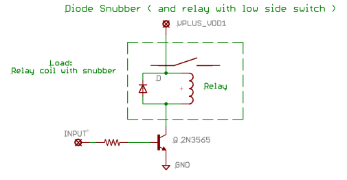
| + | Sometimes you will want to switch an external device on and off with a device that can only source a small amount of current (a microcontroller for example). For this you will need a relay. A relay is a mechanical device with a electromagnetic coil and a metal switch. When the coil is energized, the metal switch will move, completing the circuit. | ||
| − | + | An inductive element, like the relay coil, is likely to generate an undesired voltage when the current is suddenly stopped. Use a diode (snubber) to dissipate the extra voltage. | |
| − | The | + | The diode is connected in reverse from the normal voltage across the inductor, when the voltage is removed the collapsing field can continue to drive current through the diode without generating a high voltage. |
Circuit: | Circuit: | ||
| + | [[Image:diodesnubber.png | Diode snubbber ]] | ||
| + | |||
| + | Discussion: | ||
| − | + | We are assuming in this circuit that the input does not have enough output to drive the relay directly so we are using a transistor low side switch to increase the drive { see '''Low Side Switch''' on this page ). In the circuit shown, the "input" will come directly from the small current source device (microcontroller output pin). The resistor must be sized correctly, along with the NPN transistor DC current gain, to ensure sufficient current passes through the relay coil to activate it. | |
| + | |||
| + | Other inductors that might use a diode snubber are transformers, solenoids, dc motors, and of course straight ahead inductors. | ||
| + | |||
| + | More information: | ||
| − | + | *[[Relays]] | |
| − | * | + | *[http://en.wikipedia.org/wiki/Solid_state_relay Solid state relay] |
| − | * | + | *[http://en.wikipedia.org/wiki/snubber "snubber" from Wikipedia, the free encyclopedia] |
| − | * | + | *[http://en.wikipedia.org/wiki/flyback_diode "flyback diode" from Wikipedia, the free encyclopedia] |
| − | * | + | *[http://en.wikipedia.org/wiki/Relay "relay" from Wikipedia, the free encyclopedia] |
| − | * | + | *[http://www.dnatechindia.com/index.php/Tutorials/8051-Tutorial/Relay-Interfacing.html Microcontroller] relay interfacing example. |
| − | + | == Three Terminal Regulator == | |
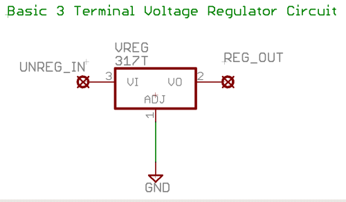
| − | + | Use when you need a regulated voltage and or short circuit protection. | |
| − | + | Most circuits run better if the primary power source is a constant fixed voltage. A battery is only a poor approximation to this. Taking a battery or other voltage source ( like a wall wart plug in transformer ) and running it through a voltage regulator transforms it into a good fixed source of voltage. It also generally adds current limiting as short circuit protection. The 7805 is a very common 5 volt regulator. | |
| − | [ | + | Circuit: |
| + | [[Image:ttr.png | Three Terminal Regulator ]] | ||
| − | + | Discussion: | |
| − | + | The circuit above is very basic. Practical circuits normally include filter capacitors on both the input and the output. Most regulators protect against both over temperature and over current. Regulators come in various voltages both positive and negative. They also vary in maximum current output. There are also adjustable regulators, ways of using regular regulators as adjustable ones, and ways of boosting the current output. The spec sheets often describe how to do these things. Voltage regulators “use up” a couple of volts of the input voltage, low drop out regulators have use less, cost more. It is a good idea to check the specification for any regulator you are going to use. The LM78xx ( positive ) and LM79xx ( negative ) are quite common. Most three terminal devices are "linear" they disappate the excess power in the input as heat, thus they are not very efficient. Switching regulators can be much more efficient, but are not normally 3 terminal devices ( although you and make it one by putting the entire circuit in a box with just 3 wires coming out ). | |
| − | + | More information: | |
| + | *[[Basic Voltage Regulators]] | ||
| + | *[http://en.wikipedia.org/wiki/7805 7805 From Wikipedia, the free encyclopedia] | ||
| + | *[http://www.tkk.fi/Misc/Electronics/circuits/psu_5v.html Simple 5V power supply for digital circuits] | ||
== Transistor Low Side Switch == | == Transistor Low Side Switch == | ||
| Line 106: | Line 396: | ||
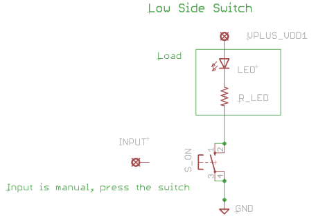
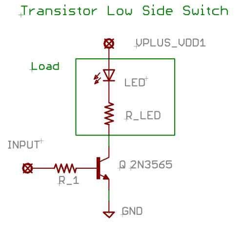
Use this circuit when you wish to turn a load on and off with both a low voltage and a low current. Note that neither side of the load is grounded. | Use this circuit when you wish to turn a load on and off with both a low voltage and a low current. Note that neither side of the load is grounded. | ||
| − | A low side switch is one which switches a circuit on and off at the ground or low side of the circuit. The advantage of a low side switch is that when using a transistor as the switch the voltage to drive the transistor is itself a low voltage. It is often the easy way to drive | + | A low side switch is one which switches a circuit on and off at the ground or low side of the circuit. The advantage of a low side switch is that when using a transistor as the switch the voltage to drive the transistor is itself a low voltage. It is often the easy way to drive LEDS, motors, and other high current devices from such low power devices as PIC output ports. Low side switches are popular and there are many integrated circuits for them as well as this circuit. |
| − | Circuit: | + | Circuit with switch: |
| + | |||
| + | [[Image:low_ss.png | Transistor Low Side Switch ]] | ||
| + | |||
| + | Circuit with transistor: | ||
| − | [[Image: | + | [[Image:Tran_lss.jpg | Transistor Low Side Switch ]] |
Where | Where | ||
| Line 120: | Line 414: | ||
| − | + | Discussion: | |
The voltage at the collector of the circuit should fall to a fraction of a volt when the input is high. To acomplish this: | The voltage at the collector of the circuit should fall to a fraction of a volt when the input is high. To acomplish this: | ||
*Compute the value of R_LED using ohms law and the specifications for the LED. | *Compute the value of R_LED using ohms law and the specifications for the LED. | ||
*Compute the current through the LED. | *Compute the current through the LED. | ||
| − | *The transistor must | + | *The transistor must sink the current, it should be equal approximately to the input voltage divided by R1 times the beta of the transistor. |
An example calculation would be nice, and will appear later. | An example calculation would be nice, and will appear later. | ||
| + | |||
| + | This circuit is sometimes called "grounded-emitter configuration". Note that this circuit can be realized with a bipolar transistor or fet. The bipolar transistor has a lower drive voltage ( usually well under 2 volts ) the fet can easily need 10 volts of drive -- use a logic level fet to reduce the drive voltage. | ||
| + | |||
| + | Some characteristics: | ||
| + | |||
| + | *Useful ( with simple circuits and common components ) for currents from a max of a few amps and voltages of 10's of volts. | ||
| + | *Can be very fast, into the Mega Hz. | ||
| + | *Can be very cheap at the low end. | ||
| + | *Small, simple. | ||
| + | *Some integrated circuit drivers like the are basically multiple transistor low side switches. | ||
| + | |||
| + | |||
| + | More Information: | ||
| + | *[http://en.wikipedia.org/wiki/Transistor#Switches Transistor From Wikipedia, the free encyclopedia] | ||
== Transistor High Side Switch == | == Transistor High Side Switch == | ||
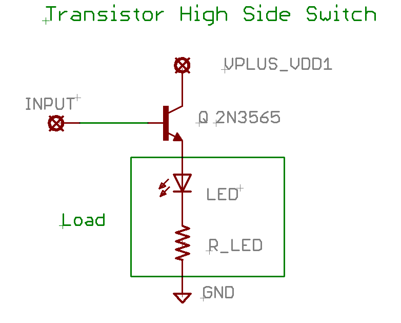
| − | Use this circuit when you wish to turn a load on and off with a voltage at a low current. Note that low | + | Use this circuit when you wish to turn a load on and off with a voltage at a low current. Note that low side of the load is grounded. The voltage to turn on the switch is equal to the supply voltage ( or perhaps just a bit larger ) |
| − | A high side switch is one which switches a circuit on and off at the supply voltage or high side of the circuit. The advantage of a high side switch is that the load is grounded on one side. Compared to the low side switch it needs a higher voltage to drive it, but it also eliminates one resistor of that circuit. It the voltage to drive it is available it may be the circuit of choice. It is often the easy way to drive leds motors and other high current devices from such low power devices as PIC output ports. | + | A high side switch is one which switches a circuit on and off at the supply voltage or high side of the circuit (the high side can be negative, it is a side away from ground). The advantage of a high side switch is that the load is grounded on one side. Compared to the low side switch it needs a higher voltage to drive it, but it also eliminates one resistor of that circuit. It the voltage to drive it is available it may be the circuit of choice. It is often the easy way to drive leds motors and other high current devices from such low power devices as PIC output ports. |
| + | |||
| + | Here is a high side switch with a push button: | ||
| + | |||
Circuit: | Circuit: | ||
| − | [[Image:tran_hss.png | Transistor High Side Switch ]] | + | [[Image:high_ss.png | High Side Switch ]] |
| + | |||
| + | |||
| + | |||
| + | Circuit with a transistor: | ||
| + | |||
| + | [[Image:tran_hss.png | Transistor High Side Switch]] | ||
| + | |||
| + | |||
Where | Where | ||
| Line 152: | Line 471: | ||
No resistor is needed into the base of the transistor because as the load draws current the voltage at the base will rise and limit the base current. The input voltage should be about equal to VPLUS_VDD, high compared to that needed for the low side switch. | No resistor is needed into the base of the transistor because as the load draws current the voltage at the base will rise and limit the base current. The input voltage should be about equal to VPLUS_VDD, high compared to that needed for the low side switch. | ||
| + | |||
| + | This high side switch usually requires the base voltage of Q to be VPLUS_VDD plus the turn-on voltage of the transistor to turn all the way on. Another approach to the high side switch that requires a lower turn-on voltage is to use a PNP transistor as the switch. The base of the PNP is pulled up to VPLUS_VDD and connected to the collector of a small signal NPN transistor, Q2. Q2's emitter is connected to ground and its base is connected to the input signal through a current limiting resistor -- now the problem is that a high voltage is required to turn the switch off. | ||
| + | |||
| + | |||
| + | === bootstrap circuit === | ||
| + | |||
| + | Often H-bridges use n-FETs in all 4 arms, to reduce cost. | ||
| + | Unfortunately, power n-FETs require a gate voltage much higher -- many power n-FETs require 10 V higher -- than both of their other two legs in order to keep them turned hard on (necessary for efficient power H-bridges). | ||
| + | Since the drain of the high-side n-FET is generally already connected to the highest voltage available from the batteries, | ||
| + | where are we going to find that even higher voltage? | ||
| + | Often we use a bootstrap circuit. | ||
| + | (see | ||
| + | Mamadou Diallo from Texas Instruments. | ||
| + | [http://www.ti.com/lit/an/slua887/slua887.pdf "Bootstrap Circuitry Selection for Half-Bridge Configurations". | ||
| + | 2018. | ||
| + | ) | ||
| + | |||
| + | Historically | ||
| + | The Intel 4004 uses a bootstrap circuit[http://insanity4004.blogspot.com/2015/10/puzzling-out-bootstrap-load_13.html] | ||
| + | which is apparently one of several reasons | ||
| + | the 4004 has a minimum clock rate (maximum cycle time). | ||
| + | Reece Pollack is translating the design to a static-logic implementation[http://insanity4004.blogspot.com/2012/09/full-circle.html]. | ||
| + | (a fully-static system makes it possible to pause the system indefinitely, | ||
| + | which is very convenient for debugging). | ||
| + | Today we have several alternatives to bootstrap circuits: | ||
| + | * If you're building digital logic out of discrete transistors, you might as well replace the 2-transistor bootstrap load circuit with an actual physical discrete resistor, which works better (?). | ||
| + | * If you're building digital logic out of FPGAs or full-custom ASICs, you're probably using CMOS -- both nFET and pFET -- and a single nFET works better than a 2-p-FET bootstrap load, and a single pFET works better than a 2-n-FET bootstrap load. | ||
| + | * If you're building a H-bridge, even today it is often better to use all-n-FET rather than both n-FET and p-FET; the bootstrap circuit gives a minimum PWM frequency (maximum PWM cycle time) and a minimum and maximum duty cycle (one step less than 100%); replacing that circuit with an independent oscillator and charge pump allows you to go all the way to 100% forward or 100% reverse. | ||
| + | |||
| + | |||
== Transistor Emitter Follower == | == Transistor Emitter Follower == | ||
| Line 159: | Line 508: | ||
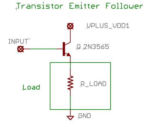
This circuit is a variation of the transistor high side switch. The difference is that we typically drive this circuit in a linear way ( all of the voltages between 0 and the supply voltage ) to make it a linear amplifier. | This circuit is a variation of the transistor high side switch. The difference is that we typically drive this circuit in a linear way ( all of the voltages between 0 and the supply voltage ) to make it a linear amplifier. | ||
| − | The emitter follower is also called a common collector circuit. | + | The emitter follower is also called a common collector circuit. The Emitter Follower is basically a high side switch, but when we call it an emitter follower we normally think of it as a linear ( analog ) amplifier, rather than as a switch. |
Circuit: | Circuit: | ||
| Line 168: | Line 517: | ||
*R_LOAD represents the resistance of the load | *R_LOAD represents the resistance of the load | ||
*Q is a npn bipolar transistor | *Q is a npn bipolar transistor | ||
| − | *VPLUS_VDD is the power supply for the | + | *VPLUS_VDD is the power supply for the Load |
The current to drive the circuit is approximately the current to drive the load divided by the beta of the transistor. Use a Darlington connected transistor for a very high beta. | The current to drive the circuit is approximately the current to drive the load divided by the beta of the transistor. Use a Darlington connected transistor for a very high beta. | ||
| Line 189: | Line 538: | ||
*[http://en.wikipedia.org/wiki/Common_collector Common collector From Wikipedia, the free encyclopedia] | *[http://en.wikipedia.org/wiki/Common_collector Common collector From Wikipedia, the free encyclopedia] | ||
| + | |||
| + | == Transistor -- Push Pull Circuit == | ||
| + | |||
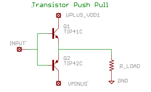
| + | Use when you need current gain and need both positive and negative output. | ||
| + | |||
| + | A modification of the “transistor emitter follower” that can give both positive and negative outputs. Based on two transistors one npn the other pnp: one pushes the other pulls. | ||
| + | |||
| + | Circuit: | ||
| + | [[Image:pptrans.png | Push Pull Transistor Circuit]] | ||
| + | |||
| + | Where | ||
| + | *Q1 transistor 1 need not be a TIP41C but does need to be NPN | ||
| + | *Q2 transistor 2 need not be a TIP42C but does need to be PNP | ||
| + | *R_LOAD represents the load, here it is in the emitter, it could also be placed in the collector circuit | ||
| + | *VPLUS_VDD Power supply voltage, positive. | ||
| + | *VMINUS Power supply voltage, negative. | ||
| + | |||
| + | Discussion: | ||
| + | Often there are other components for transistor bias or other purposes. The circuit here is really basic. The common transistors used are so called complementary pairs, similar characteristics but one npn and the other pnp. Note that we need both positive and negative power supplies. You can also put the push pull circuit inside the feedback loop of an op amp to get a high current op amplifier. Push pull amplifies can also be made with other types of transistors, tubes, or other components. | ||
| + | |||
| + | More information: | ||
| + | *[http://www.ecircuitcenter.com/Circuits/pushpull/pushpull.htm Push-Pull Output Stage] | ||
| + | *[http://www.allaboutcircuits.com/vol_6/chpt_6/10.html Class B audio amplifier] | ||
| + | *[http://en.wikipedia.org/wiki/Electronic_amplifier Electronic amplifier From Wikipedia, the free encyclopedia (search on Class B and AB )] | ||
| + | |||
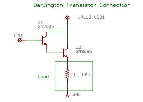
| + | == Transistors -- Darlington connected == | ||
| + | |||
| + | Use a Darlington transistor connection when you want really high current gain. Gain of 1000 is easily in reach. That is 1 ma to 1 amp | ||
| + | This is a useful connection of 2 transistors that together form a transistor of much larger gain. You can also buy Darlington transistors all packaged in a single case with just 3 connections exposed to the outside. | ||
| + | |||
| + | Circuit: | ||
| + | [[Image:dtrans.png | Darlington Transistor Connection ]] | ||
| + | |||
| + | Where | ||
| + | *Q1 transistor 1 need not be a 2N3565 but does need to be NPN | ||
| + | *Q2 transistor 2 need not be a 2N3565 but does need to be NPN | ||
| + | *R_LOAD represents the load, here it is in the emitter, it could also be placed in the collector circuit | ||
| + | *VPLUS_VDD Power supply voltage, positive. | ||
| + | |||
| + | Discussion: | ||
| + | |||
| + | Often Q1 is a high gain small signal transistor and Q2 a lower gain power transistor. You can use PNP transistors by using a negative power supply. Use a ULN2803 ( or similar chips ) to get 8 darlingtons in one package, useful as low side switches and in conjunction with microcontrollers. | ||
| + | * The above diagram shows a high side switch, but other transistor configurations can also be used. | ||
| + | * PNP transistors can also be used, the important point is that both transistors be of the same type. | ||
| + | |||
| + | More information: | ||
| + | *[http://en.wikipedia.org/wiki/Darlington_transistor Darlington transistor From Wikipedia, the free encyclopedia] | ||
| + | *[http://www.kpsec.freeuk.com/trancirc.htm Transistor Circuits ( search on Darlington )] | ||
| + | *[http://www.ibiblio.org/kuphaldt/electricCircuits/Semi/SEMI_4.html Lessons In Electric Circuits -- Volume III Chapter 4 BIPOLAR JUNCTION TRANSISTORS Darlington pair ( search on Darlington )] | ||
| + | |||
| + | == Transistors -- Sziklai pair == | ||
| + | |||
| + | Similiar in use to a Darlington transistor connection when you want really high current gain. Gain of 1000 is easily in reach. That is 1 ma to 1 amp This is a useful connection of 2 transistors that together form a transistor of much larger gain. Unlike a Darlington the transistors are of opposite types. The circuit also has some other differences in detail, see the refrences. | ||
| + | |||
| + | Circuit: | ||
| + | [[Image:sptrans.png | Sziklai pair ]] | ||
| + | |||
| + | Where | ||
| + | *Q1 transistor 1 need not be a xxx but does need to be NPN | ||
| + | *Q2 transistor 2 need not be a xxx but does need to be PNP | ||
| + | *R_LOAD represents the load, here it is in the emitter, it could also be placed in the collector circuit | ||
| + | *VPLUS_VDD Power supply voltage, positive. | ||
| + | |||
| + | Discussion: | ||
| + | |||
| + | Often Q1 is a high gain small signal transistor and Q2 a lower gain power transistor. You can use PNP transistors by using a negative power | ||
| + | |||
| + | More information: | ||
| + | *[http://en.wikipedia.org/wiki/Sziklai_pair Sziklai pair From Wikipedia, the free encyclopedia] | ||
| + | |||
| + | |||
| + | |||
| + | == RC Filter == | ||
| + | |||
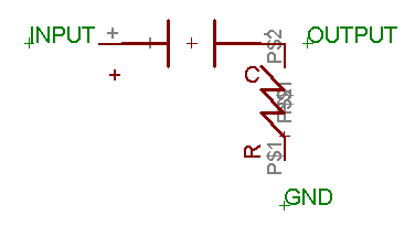
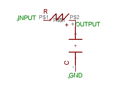
| + | The most basic filters are the RC-High Pass and RC-Low Pass filters. The high pass filter removes DC and low frequencies and the low pass removes high frequencies. | ||
| + | |||
| + | |||
| + | '''High Pass''' [[Image:rchighpass.png | RC High Pass Filter]] | ||
| + | '''Low Pass''' [[Image:rclowpass.png | RC Low Pass Filter]] | ||
| + | |||
| + | Both circuits have the same 3dB frequency or the frequency at which the power of the signal is aproximately halved. | ||
| + | |||
| + | <math> | ||
| + | f_\mathrm{c} = {1 \over 2 \pi \tau } = {1 \over 2 \pi R C} | ||
| + | </math> | ||
| + | |||
| + | The way to remember the two circuits is to think about how the capacitor acts at various signal frequencies. At high frequencies capacitors act like wires. At low frequencies capacitors act like disconnections. | ||
| + | |||
| + | An important use of low pass filters is for the anti-aliasing circuity on the input of an A/D converter or the output of a D/A converter. An important use of a high pass filter is to remove the DC offset of a signal. For example, it's possible to use a power supply that is +5 to GND to generate a sin from a D/A converter and use a high pass filter to change the sin to a +2.5 to -2.5 signal at the output. | ||
| + | |||
| + | More information: | ||
| + | *[http://en.wikipedia.org/wiki/Low-pass_filter Low Pass Filter] | ||
| + | *[http://en.wikipedia.org/wiki/High-pass_filter High Pass Filter] | ||
| + | *[http://www.tonnesoftware.com/elsie.html The Windows ® program for electrical filter design and network analysis] | ||
| + | |||
| + | == Series Circuit == | ||
| + | |||
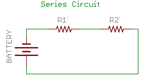
| + | In a series circuit the current first flows through one component then another and so on. The key to these circuits is that the current is the same in every element of the circuit and the total of the voltage across each of the components adds up to the voltage of the battery. A current meter is always in series with the part of the circuit whose current is being measured. | ||
| + | |||
| + | Circuit: | ||
| + | [[Image:series.png | Series Circuit ]] | ||
| + | |||
| + | Where | ||
| + | *R1 resistor 1 or any other 2 terminal component, capacitor, inductor, diode.... | ||
| + | *R2 resistor 2 or any other 2 terminal component..... | ||
| + | *BAT a battery or other voltage source | ||
| + | |||
| + | I you have a lot of components that use the same current put them in series. This is often how LEDs are connected to higher voltages; this also eliminates the need for a current limiting resistor on each LED. With a bit of math you can show that the two resistors act like one resistor of value R = R1 + R2 . When you need a resistor of a different value than you have you can sometimes “make it up” using a series connection of resistors you do have. Two identical resistors in series are equivalent to one of double the resistance. A series circuit can have more than 2 resistors, there can be 3, 4, ... You can find out more about series circuits in the references. This circuit should be contrasted with the Parallel Circuit. A voltage divider is an example of a series circuit. | ||
| + | |||
| + | More information: | ||
| + | * [http://en.wikipedia.org/wiki/Parallel_circuit Series and parallel circuits From Wikipedia, the free encyclopedia] | ||
| + | |||
| + | <!---------------------------------------------------------------------> | ||
| + | |||
| + | ==Seven segment LEDs== | ||
| + | Use these to display number to a user. | ||
| + | |||
| + | *[http://chungyan5.no-ip.org/vc/trunk/AltiumDesigner6ProjectFiles.zip?root=7segment_LEDs&view=log AltiumDesigner6ProjectFiles] | ||
| + | *[http://www.dnatechindia.com/index.php/Tutorials/8051-Tutorial/7-Seg-Interfacing.html Interfacing Seven Segment to Microcontroller] | ||
| + | i need a clear explanation about schmitt trigger and also need the operation details about that circuit...if i give the input of the schmitt trigger is 0v means what is the output of the circuit? | ||
| + | |||
| + | == Oscillators == | ||
| + | |||
| + | [[Image:Flip-flop circuit.jpg]] | ||
| + | (is there a better page to discuss oscillators?) | ||
| + | |||
| + | == Power up low active reset circuit == | ||
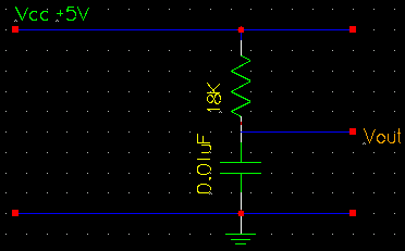
| + | Use this circuit with a microcontroller to keep it in reset for a short period of time after the power supply is turned on. Some microcontrollers like this kind of start up. Note that this is really just an application of the RC Filter, also on this page. | ||
| + | |||
| + | |||
| + | [[Image:power_up_low_active_reset_circuit.png]] | ||
| + | [[Image:pular.png]] | ||
| + | *[http://chungyan5.no-ip.org/open_data/electronic_computer/middleware/pwr_up_low_active_reset/ power_up_low_active_reset_circuit] | ||
| + | *[http://spreadsheets.google.com/pub?key=pobKDna9aVYeKjbR-Hf-OIg Result of Resistant to delay time] | ||
| + | |||
| + | == ADC Voltage Protection Circuit == | ||
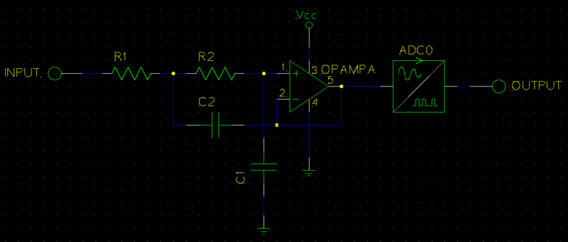
| + | The input to an Analog to Digital Converter (ADC) has some issues that need a bit of attention. | ||
| + | The ADC can be damaged by input voltages that are too high or too low. | ||
| + | An op-amp is the best way to protect the ADC. | ||
| + | (Additionally, an opamp circuit can provide amplification (although this example doesn't); it can remove aliasing noise; and it drives the ADC with low impedance, which can be quite helpful). | ||
| + | |||
| + | This Sallen-Key filter is a specialization of '''Op amp Non Inverting Amplifier''' also on this page. | ||
| + | |||
| + | [[Image:Adc.png|thumb|800px|center]] | ||
| + | *This opamp circuit is used to | ||
| + | #provide a low input source resistance to the ADC | ||
| + | #protect ADC. Even when the input signal exceeds the supply/reference voltage (i.e. INPUT > V<sub>cc</sub>), the voltage into the ADC input pin is capped at the supply voltage. | ||
| + | *Requirement for the op-amp: | ||
| + | **The op-amp can withstand the input signal beyond the supply voltage, provided that the input current is limited to I<sub>max</sub> (e.g. [http://focus.ti.com/lit/ds/symlink/opa4340.pdf OPA4340] I<sub>max</sub> = 10mA) | ||
| + | **To reduce noise picked up from the op-amp, use an op-amp with a low Input Voltage Noise Density (measured in nV/√Hz) | ||
| + | |||
| + | *Test conditions: | ||
| + | **V<sub>signal</sub> = 5V | ||
| + | **R1 = 8.2kohm, R2 = 15kohm, C1 = 0.1uF, C2 = 0.22uF | ||
| + | **Measured V+ = 3.8V | ||
| + | **Calculated current = (5-3.8)/23200 = 52uA < 10mA | ||
| + | |||
| + | More Information: | ||
| + | * [[input protection]] circuits | ||
| + | * [http://en.wikipedia.org/wiki/Sallen_Key_filter Wikipedia: "Sallen–Key topology"] | ||
| + | * [http://en.wikipedia.org/wiki/anti-aliasing Wikipedia: "anti-aliasing"] and [http://en.wikipedia.org/wiki/anti-aliasing_filter Wikipedia: "anti-aliasing filter"]] | ||
| + | |||
== Voltage Divider == | == Voltage Divider == | ||
| Line 210: | Line 721: | ||
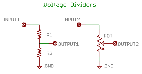
The equation assumes that the input source is low impedance and the output is high impedance, if this is not true consider using a buffer on the input or the output ( Op Amp Unity Gain Buffer or Transistor Emitter Follower ) For audio applications a so called “log taper” pot may be used as it better matches the way in which we hear. If you want a calibrated control you may use a precision “10 turn precision” pot. | The equation assumes that the input source is low impedance and the output is high impedance, if this is not true consider using a buffer on the input or the output ( Op Amp Unity Gain Buffer or Transistor Emitter Follower ) For audio applications a so called “log taper” pot may be used as it better matches the way in which we hear. If you want a calibrated control you may use a precision “10 turn precision” pot. | ||
| − | |||
More information: | More information: | ||
*[http://www.seattlerobotics.org/encoder/mar97/basics.html Very Basic Circuits] | *[http://www.seattlerobotics.org/encoder/mar97/basics.html Very Basic Circuits] | ||
| + | *[http://itp.nyu.edu/physcomp/sensors/Schematics/VoltageDivider Voltage Divider] | ||
| + | |||
| + | == Voltage Divider using a Light Dependent Resistor == | ||
| + | |||
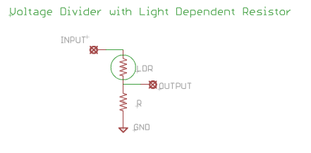
| + | Used to generate a voltage that depends upon light level. With the LDR on the "high side" the voltage will go up when the amount of light goes up. | ||
| + | You need to use a resistor in series with the light dependent resistor, this combination lets a variable current flow through the circuit. The voltage across the resistor will vary with the light brightness ( so will the voltage across the LDR, the two will total the input voltage. ) What size resistor should you use? A rule of thumb: Put the LDR in medium brightness and measure its resistance with a ohm meter. Use that value resistor then in medium light you will get 1/2 the input voltage at the output. | ||
| + | |||
| + | Circuit: | ||
| + | |||
| + | |||
| + | [[File:VdivideLDR.png]] | ||
| + | |||
| + | Where | ||
| + | |||
| + | *Input = 5v from power supply Vcc | ||
| + | *Output = signal to connect what ever addition circuit | ||
| + | *LDR The Light dependent resistor | ||
| + | *R: A resistor as described above. | ||
| + | |||
| + | == Wheatstone Bridge == | ||
| + | '''Draft''' | ||
| + | Use this circuit when you want to measure the value of a resistor or detect a small change in resistance. | ||
| + | |||
| + | Circuit: | ||
| + | [[Image:wbridge.png | Wheatstone Bridge ]] | ||
| + | |||
| + | Where | ||
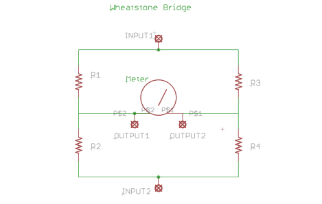
| + | *Input1 Input 1 normally + DC | ||
| + | *Input2 Input 2 normally - DC or ground. | ||
| + | *R1 Resistor 1. | ||
| + | *R2 Resistor 2. | ||
| + | *R3 Resistor 3. | ||
| + | *R4 Resistor 4. | ||
| + | *Output1 Output 1 for null reading. | ||
| + | *Output2 Output 2 for null reading. | ||
| + | *Meter Use to detect meter balance = null = 0 reading. | ||
| + | |||
| + | Discussion: | ||
| + | |||
| + | The circuit is basically two voltage dividers with the output taken across the output of each voltage divider. It is in "balance" when the output is 0. This is true when R1/R2 = R3/R4. The output traditionally went to a galvanometer a very high sensitivity meter. Input traditionally was a battery. By using calibrated resistors for R1, R2, and R3 the value of R4 may easily be calculated. The whole circuit including a wide range of precision resistors, the battery and galvanometer was all packaged in an box and sold as a unit. The same principal can be used with components other than resistors and AC for input instead of DC. | ||
| + | |||
| + | More Information: | ||
| + | *[http://itp.nyu.edu/physcomp/sensors/Schematics/WheatstoneBridge Wheatstone Bridge] | ||
| + | *[http://physics.kenyon.edu/EarlyApparatus/Electrical_Measurements/Capacitance_Bridge/Capacitance_Bridge.html Capacitance Bridge] This one is an antique. | ||
| + | |||
| + | == current mirror == | ||
| + | |||
| + | (FIXME: fill in details) | ||
| + | |||
| + | [[Wikipedia: current mirror]] http://en.wikipedia.org/wiki/Current_mirror | ||
| + | |||
| + | == Further Reading == | ||
| + | |||
| + | * [http://freecircuitdiagram.com/ FreeCircuitDiagram] Lots of circuits, not always so basic, more like projects, but many are quite simple. Some but not elaborate explanation of the circuit. | ||
| + | |||
| + | |||
| + | == General Comments == | ||
| + | |||
| + | ''... do we need another page for not-so-basic circuits such as the Baker clamp ? ...'' I looked it up and would say it is not so basic. So perhaps [[Not So Basic Circuits]] would be a good place to put such things. What do others think? russ_hensel | ||
| − | + | More not-so-basic circuits: | |
| + | [http://www.geofex.com/circuits/what_are_all_those_parts_for.htm "What are all those parts for??"] by R.G. Keen. 2002 | ||
| + | shows a "simple" noninverting gain circuit, | ||
| + | and explains what all the "extra" parts do. | ||
| − | + | * Philip C. Todd. "Snubber Circuits: Theory , Design and Application". 1993. [http://www.ti.com/lit/an/slup100/slup100.pdf] has more complex snubber circuits. | |
| + | * [http://electronics.stackexchange.com/questions/17731/choosing-components-for-a-triacs-snubber "Choosing components for a triac's snubber"] has more complex snubber circuits. | ||
| − | |||
| − | + | [[Category:Components]][[Category:Schematics]] | |
Latest revision as of 22:48, 9 August 2022
These are circuits and parts of circuits that we see over and over again in larger projects. Understanding a complex circuit is much easier if you understand these building blocks.
Operational amplifier are the basis for many circuit building blocks especially in the range of DC to 1 meg Hz. See OpAmp Links.
Contents
- 1 Introduction and Page Status....
- 2 Amplifiers
- 3 Current Sense Resistor ( Shunt Resistance )
- 4 Current Limit or Constant Current ( Transistor Based )
- 5 Filter Capacitor / Decoupling Capacitor / Low Pass Filter
- 6 High Side Switch
- 7 Light Emitting Diode ( with current limiting resistor )
- 8 Op Amp Non Inverting Amplifier
- 9 Op Amp Precision Rectifier
- 10 Op amp Unity Gain Buffer
- 11 Parallel Circuit
- 12 Pull Up and Switch
- 13 Pull Down and Switch
- 14 Rectifier - Power
- 15 Rectifier - Signal and Absolute Vaue Circuit
- 16 Relay with Diode Snubber
- 17 Three Terminal Regulator
- 18 Transistor Low Side Switch
- 19 Transistor High Side Switch
- 20 Transistor Emitter Follower
- 21 Transistor -- Push Pull Circuit
- 22 Transistors -- Darlington connected
- 23 Transistors -- Sziklai pair
- 24 RC Filter
- 25 Series Circuit
- 26 Seven segment LEDs
- 27 Oscillators
- 28 Power up low active reset circuit
- 29 ADC Voltage Protection Circuit
- 30 Voltage Divider
- 31 Voltage Divider using a Light Dependent Resistor
- 32 Wheatstone Bridge
- 33 current mirror
- 34 Further Reading
- 35 General Comments
Introduction and Page Status....[edit]
( Some of schematics have been drawn in Eagle and the screen captured, use other methods if you wish. Feel free to add your own circuits, as long as they are basic building blocks, there are lots of other places for project circuits. If you get into more advanced circuits, give them their own page and link to them. Some entries are not complete, if the explanation of the circuit does not match the diagram that is a good tip off. )
To Do
- Why not put alpha order?
- work on external links
More circuits that would be good to add
- AC Coupling Capacitor / High Pass Filter
- Battery Lamp and Switch
- Diode Rectifier
Current rating and full wave rectification
- LM35 Temperature Sensor
- 555 Timer astable oscillator
- current mirror
- Transistor Current Mirror
- charge pump
- diode for forward drop bias voltage
- diode logical or
- H Bridge
An H bridge is an electronic circuit that causes current to flow in one direction or the other ( from a single ended power supply ). Often used for motor control motor driver. It is an electronic double pole double throw switch.
- [1] See Section on H-Bridge
- H-Bridge Fundamentals
- integrator
- diode full wave bridge
- RC timer
- RF Mixers
- diode rounding circuit
- row and collumn connection
- sample and hold http://en.wikipedia.org/wiki/Sample_and_hold
- Simple Oscillator circuits
- transformer
- voltage multiplier and voltage doubler
Links to basic circuits:
- Donny's Learn Electrical Engineering for Beginners
- DC/AC Circuit Reference
- Educypedia A web site of links. Lots of material.
Amplifiers[edit]
An amplifier is any circuit which has a larger output than input, typically either larger voltage or larger current, or both. Generally larger power out than in. Several of the circuits here are amplifiers, but as these are only basic circuit, many types of amplifiers are omitted here.
See the sections on: Op amp Non Inverting Amplifier, Op amp Unity Gain Buffer ....
Current Sense Resistor ( Shunt Resistance )[edit]
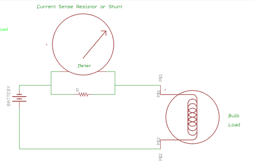
A current Sense Resistor is a low value of resistor that is placed in series with some other circuit. We can then measure the voltage across the resistor to compute the current. If the resistor has a low value compared to other components we can ignore the effect on the circuit. We use the word shunt when the voltage is measured by a device that has a fairly low resistance itself. We then have to do a more careful calculation of how the current is shared by the two devices.
Where
- R shunt resistor used to sense the current ( and divert it from the meter ). Usually much less in value than the internal resistance of the meter.
- METER meter or other device used to measure the voltage across the shunt resitor. Often the resistance of the meter is ignored ( if high ).
- BATTERY a battery or other voltage source.
- BULB an incandescent light bulb
Discussion:
In the old days a sensitive meter, say 50 mv full scale, would be used with a set of shunt, some looking like metal bars, to measure a wide range of currents, up to and exceeding 50 amps. Sometimes a meter came with a set of shunts for measuring different currents. See links. A completely different way to measure currents is to use a hall effect sensor.
Links to More information:
- Scienceshareware.com's How A Precision Resistor Is Used to Measure / Calculate Current and Power in an Electrical Circuit.
- High-Side Current-Sense Measurement: Circuits and Principles
- Shunt (electrical) From Wikipedia, the free encyclopedia
- Other ways to measure current: Motor_driver#current_sense
Current Limit or Constant Current ( Transistor Based )[edit]
This is a modification of the emitter follower to limit the current output. So if your output stage is an emitter follower you can add current limiting to it. Or given enough input drive, say from a voltage divider it will act as a constant current source.
Circuit:
Where
- R1 base resistor to limit base current to transistor Q1.
- R2 current sense resistor used to sense the current and turn on transistor Q2.
- Q1 main transistor supplying the load current.
- Q2 current limiting transistor.
Discussion:
The idea here is that R2 is a current sense resistor. When the sense voltage across R2 reaches about .7 ( for silicon transistors ) Q2 begins to conduct and diverts the base drive from Q1 cutting its output current. So the max. current from the circuit is reached when I*R2 = .7. This circuit can be used to protect amplifiers ( including push pull amps. ), power supplies and other circuits; or it can be used as a constant current circuit. It is not a precision circuit, but it is cheap, simple, and effective circuit.
More information:
- Variable (Adjustable) Current Limiter Circuit This is a bit more complicated version using a transistor to drive a darlington transistor, with the limit being adjustable.
- Current Source for Resistance Measurement
- The Problem with Current Limit Discusses this circuit as applied to a power amplifier.
- Constant current LED-Tester Simple application of the circuit as an LED tester.
Filter Capacitor / Decoupling Capacitor / Low Pass Filter[edit]
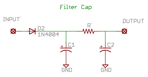
Where
- D2 is a diode, it lets current pass only in the direction of the arrow.
- R resistor
- Input a source of alternating current ( occasionally DC in which case the whole circuit serves only to protect against a reverse connection.
C1 the first, main, filter capacitor. C2 the second filter capacitor.
Discussion: In this circuit C1 is a classic filter capacitor it charges while the diode conducts, it discharges and supplies current when the diode does not. R and C2 are a second stage filter. With R set to 0, it simply adds to the value of C1. With R in the circuit it forms a low pass filter which helps remove the ripple from the power ( at the cost of some voltage drop ). In the old days R would often be a low value inductor which had a similar effect without the voltage drop. A capacitor alone is often put across a circuit component that uses power to supply bursts of current and stop noise from being propagated through the power supply.
The amount of ripple in a simple circuit like this can be determined from the supply frequency voltage, output current, and the capacitance. The amount of time without any input voltage is 1/2f. Given an output current I, the charge transferred is is I/2f. The voltage sag is then just the charge divided by the capacitance, or I/2fC. An inductor added to this circuit will compensate for voltage sag by inducing a voltage if the current starts to drop.
High Side Switch[edit]
This circuit switches a load at the high side away from ground. With a simple switch it is easy, just wire the switch into the high side. Using transistors is not so easy. There are integrated circuits that make it easy again. But this is not a basic circuit. Contrast with Transistor Low Side Switch
Light Emitting Diode ( with current limiting resistor )[edit]
Use this circuit to light low power LEDs
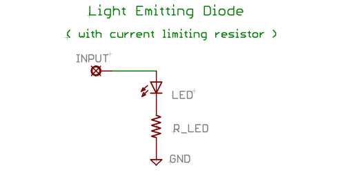
A light emitting diode can be very sensitive to small voltage changes, just a bit too much voltage and the LED will draw too much current and “burn out”. Thus it is often used with a resistor in series. If we have a 5 volt source of voltage and an LED that is specified for 2.5 volts at 10 ma, then the resistor must have ( 5 – 2.5 ) volts = 2.5 volts and 10 ma. Using ohms law 2.5/10 x 10 ee-3 = 250 ohms.
A transistor low or high side switch can be used with the resistor if your input cannot supply enough current for the LED.
Where
- LED the LED
- R_LED the current limiting resistor
- INPUT voltage source for lighting the LED
More information:
- Very Basic Circuits
- Learning About Transistors and LEDs
- WELCOME TO QUANTSUFF'S CIRCUIT PAGE. Low Voltage, high-efficiency Drivers for LED Lights
- Interfacing LED to 8051 Microcontroller
- Some thoughts on throwies interesting notes on the resistor normally used with an LED.
Op Amp Non Inverting Amplifier[edit]
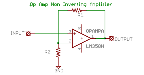
Use this circuit where the signal you have is not as large as you want, or cannot provide enough current. It is called non inverting because a positive input produces a positive output ( An inverting amplifier produces a negative output when given a positive input ).
Where
- R1 resistor 1 or any other 2 terminal component, capacitor, inductor, diode....
- R2 resistor 2 or any other 2 terminal component.....
OPAMPA Any general purpose op amp, often connected to + and - power supplies
Discussion: Gain is = ( R1/R2 ) + 1
More Information:
Op Amp Precision Rectifier[edit]
Draft - Incomplete Use this circuit where you wish to get very accurate rectification. Precision means that most of the usual forward voltage drop of a diode circuit goes away. Results look good down into the mv range.
Circuit:
Op Amp Precision Rectifier
Where
- D1 Diode....
- R2 resistor 2 or any other 2 terminal component.....
OPAMPA Any general purpose op amp, often connected to + and - power supplies
Discussion: more comming
Th
More Information:
Op amp Unity Gain Buffer[edit]
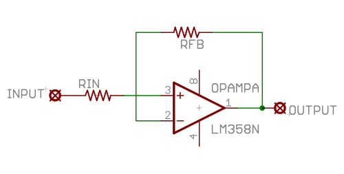
Use this circuit when you have a signal of high impedance ( can supply only a little current ) that you want to connect to another circuit that draws a significant current ( up to about 10 ma for the typical op amp. ). For example if you wish to measure the output of a voltage divider with a 0 to 1 ma meter a unity gain buffer might be just what you need. This circuit is also know as a voltage follower.
The unity gain buffer has an output voltage just the same as the input voltage. The advantage is that the input circuit does not “feel” the output. That is the input acts pretty much like a very large resistor ( many mega ohms or more ) connected to ground, and the output supplies whatever current ( up to about 10 ma ) is necessary to maintain the output voltage. Here is the circuit:
Circuit:
Where
- INPUT the input signal you wish to buffer
- RIN the input resistor, often 0 ohms.
- OPAMPA Any general purpose op amp, often connected to + and - power supplies
- RFB the feed back resistor
- OUTPUT the output
Discussion: The values of RIN and RFB are not very critical and are normally 0 ohms, just a straight connection. The op amp here is a quad or 4 op amp part, we are using just one section of it. Power needs to be supplied to pin 8 and 4 in the usual way for op amps. This circuit uses very large feedback (unity) and for this reason has poor stability margins. This may cause the output to go into oscillations when connected to certain loads (typically capacitive). Check the datasheet of individual opamps for details and remedies.
More information:
- OpAmp Links
- Buffer amplifier From Wikipedia, the free encyclopedia
- Operational Amplifiers
- Op-Amp Buffer
Parallel Circuit[edit]
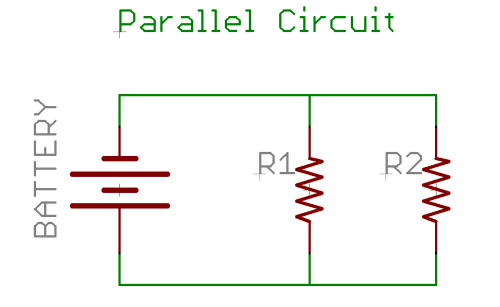
In a parallel circuit the current divides and some flows through each component . The key to these circuits is that the voltage is the same in every element of the circuit and the total of the current through each of the components adds up to the total current from the battery. When you use a current meter it is always placed in series with the part of the circuit where you wish to measure the current.
Where
- R1 resistor 1 or any other 2 terminal component, capacitor, inductor, diode....
- R2 resistor 2 or any other 2 terminal component.....
- BATTERY a battery or other voltage source
Discussion:
I you have a lot of components that use the same voltage put them in parallel. This is how most lights in a house are wired. Each individual light can be turned on and off without changing the current or voltage in the other lights. With a bit of math you can show that the two resistors act like one resistor of value R = (R1*R2)/(R1 + R2). When you need a resistor of a different value than you have you can sometimes “make it up” using a parallel connection of resistors you do have. Two identical resistors in parallel are equivalent to one of half the resistance. A parallel circuit can have more than 2 resistors, there can be 3, 4, ... You can find out more about parallel circuits in the references. This circuit should be contrasted with the Series Circuit. Parallel circuits can also be used with other components, the equations vary, for capicators the capacitances add in a parallel circuit.
More information:
Pull Up and Switch[edit]
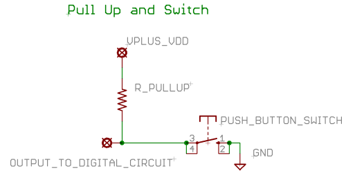
Use this circuit when you want to feed a user input to a digital circuit, for example a PIC input pin.
A pull up is a fairly high value resistor (say 1 to 100 K ohms) that is connected to the positive side of the power supply. This makes the other end of the resistor the same voltage as the power supply (as long as it is connected to a high impedance). The other end of the resistor is connected to a switch that is then connected to ground. When the switch is connected current flow through the resistor drops the entire power supply voltage and the input voltage for the circuit is now 0 (sometimes called active low, since when the switch is active the output is low). Note that a pull up ( just the resistor to V+ ) might be considered a basic circuit by itself. Pull up is sometimes used without the switch to keep a signal high all the time. It can also be connected to any other circuit or component that has ( sometimes ) a much lower impedance than the pull up and can thus force the voltage low.
Circuit:
Where
- PUSH_BUTTON_SWITCH is a push button switch
- R_PULLUP is the pull up resistor
- VPLUS_VDD is the power supply voltage
More information:
Debouncing Discussion:
We have two groups of solution: Hardware Debouncing Circuit and Software Debouncing Driver
Hardware Debouncing Circuit:
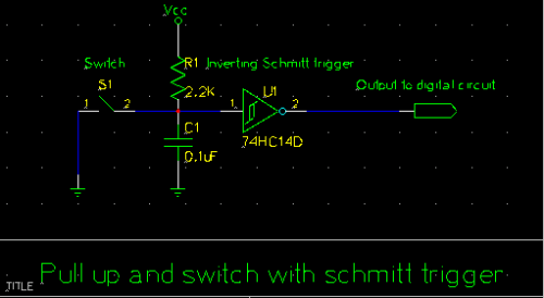
- Advantage - Do not occupy the CPU processing power for debouncing, lets CPU to handle more other application task(s)
- Disadvantage - we need to implement the above hardware circuit inside the project
Software Debouncing Driver:
- Advantage - Saving cost & space for nothing debouncing circuit
- Disadvantage - Utilize CPU processing power for debouncing, less time for CPU to handle other application process
ToDo[edit]
- Software Debouncing Driver
- compile time parameters:
- time delay between each sample
- no. of sample - until all samples
- different type of switches, may be have different above compile time parameters
- API to OS or GUI
- compile time parameters:
Pull Down and Switch[edit]
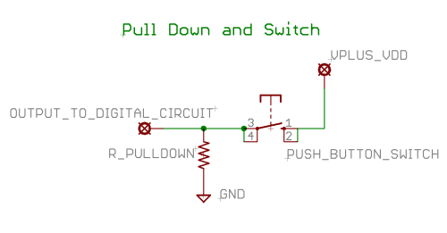
Use this circuit when you want to feed a user input to a digital circuit, for example a PIC input pin. ( like the Pull Up and Switch )
Essentially a Pull Up and Switch "upside down". A pull down is a fairly high value resistor (say 1 to 100 K ohms) that is connected to the ground side of the power supply. This makes the other end of the resistor ground as well. (as long as it is connected to a high impedance). The other end of the resistor is connected to a switch that is then connected to positive side of the power supply. When the switch is connected current flow through the resistor raises the voltage to the digital circuit to entire power supply voltage the input is now 1 (sometimes called active high, since when the switch is active the output is high ). Pull down is sometimes used without the switch to keep a signal low all the time.
Where
- R_PULLDOWN resistor which normally keeps the output low ( ground ).
- PUSH_BUTTON_SWITCH switch to make the output high
- VPLUS_VDD a battery or other voltage source
Discussion: Just a variation on the Pull Up and Switch.
Links:
* Roguescience Arduino Tutorials 4.2 Pull-up/down resistors, debouncing
Rectifier - Power[edit]
this is a stubb, almost no useful content
Use this circuit when you want to convert AC to DC at significant current in order to provide DC power to another circuit component, it can be also used as a very low precision "precision rectifier". Basically similar circuits are sometimes used as demodulators for AM signals.
Discussion:
There are many variations of this circuit, sometimes in combination with center tapped transformers, sometimes with multiple diodes ( as in bridge circuits ).
Rectifier - Signal and Absolute Vaue Circuit[edit]
this is a stubb, almost no useful content
Use this circuit when you want to know the peak voltage of an AC of time varying DC voltage of just its absolute value. It typically differes from a power rectifier in that the circuit needs its own source of power, it does not pass thru the power of the input voltage, it also differes in that the typical voltage drop of the power diode ( in the range of .5 to 2 volts ) is largely eliminated. This is a signal processing circuit.
Discussion: There are a ton of ways to do this a common way is to include a diode with a forward voltage drop in the feedback loop of an operational amplifier. There are lots of circuits that can be used, see links for discussion of different circuits and there advantages and dis.
Links:
* More Value from Your Absolute Value Circuit—Difference Amplifier Enables Low-Power, High-Performance Absolute Value Circuit
* PRECISION ABSOLUTE VALUE CIRCUITS By David Jones (520) 746-7696, and Mark Stitt
* Images
Relay with Diode Snubber[edit]
Sometimes you will want to switch an external device on and off with a device that can only source a small amount of current (a microcontroller for example). For this you will need a relay. A relay is a mechanical device with a electromagnetic coil and a metal switch. When the coil is energized, the metal switch will move, completing the circuit.
An inductive element, like the relay coil, is likely to generate an undesired voltage when the current is suddenly stopped. Use a diode (snubber) to dissipate the extra voltage.
The diode is connected in reverse from the normal voltage across the inductor, when the voltage is removed the collapsing field can continue to drive current through the diode without generating a high voltage.
Discussion:
We are assuming in this circuit that the input does not have enough output to drive the relay directly so we are using a transistor low side switch to increase the drive { see Low Side Switch on this page ). In the circuit shown, the "input" will come directly from the small current source device (microcontroller output pin). The resistor must be sized correctly, along with the NPN transistor DC current gain, to ensure sufficient current passes through the relay coil to activate it.
Other inductors that might use a diode snubber are transformers, solenoids, dc motors, and of course straight ahead inductors.
More information:
- Relays
- Solid state relay
- "snubber" from Wikipedia, the free encyclopedia
- "flyback diode" from Wikipedia, the free encyclopedia
- "relay" from Wikipedia, the free encyclopedia
- Microcontroller relay interfacing example.
Three Terminal Regulator[edit]
Use when you need a regulated voltage and or short circuit protection.
Most circuits run better if the primary power source is a constant fixed voltage. A battery is only a poor approximation to this. Taking a battery or other voltage source ( like a wall wart plug in transformer ) and running it through a voltage regulator transforms it into a good fixed source of voltage. It also generally adds current limiting as short circuit protection. The 7805 is a very common 5 volt regulator.
Discussion:
The circuit above is very basic. Practical circuits normally include filter capacitors on both the input and the output. Most regulators protect against both over temperature and over current. Regulators come in various voltages both positive and negative. They also vary in maximum current output. There are also adjustable regulators, ways of using regular regulators as adjustable ones, and ways of boosting the current output. The spec sheets often describe how to do these things. Voltage regulators “use up” a couple of volts of the input voltage, low drop out regulators have use less, cost more. It is a good idea to check the specification for any regulator you are going to use. The LM78xx ( positive ) and LM79xx ( negative ) are quite common. Most three terminal devices are "linear" they disappate the excess power in the input as heat, thus they are not very efficient. Switching regulators can be much more efficient, but are not normally 3 terminal devices ( although you and make it one by putting the entire circuit in a box with just 3 wires coming out ).
More information:
- Basic Voltage Regulators
- 7805 From Wikipedia, the free encyclopedia
- Simple 5V power supply for digital circuits
Transistor Low Side Switch[edit]
Use this circuit when you wish to turn a load on and off with both a low voltage and a low current. Note that neither side of the load is grounded.
A low side switch is one which switches a circuit on and off at the ground or low side of the circuit. The advantage of a low side switch is that when using a transistor as the switch the voltage to drive the transistor is itself a low voltage. It is often the easy way to drive LEDS, motors, and other high current devices from such low power devices as PIC output ports. Low side switches are popular and there are many integrated circuits for them as well as this circuit.
Circuit with switch:
Circuit with transistor:
Where
- LED is a low power LED
- R_LED is a current limiting resistor for the LED
- Q is a bipolar transistor
- R_1 is a current limiting resistor transistor base current
- VPLUS_VDD is the power supply for the LED
Discussion:
The voltage at the collector of the circuit should fall to a fraction of a volt when the input is high. To acomplish this:
- Compute the value of R_LED using ohms law and the specifications for the LED.
- Compute the current through the LED.
- The transistor must sink the current, it should be equal approximately to the input voltage divided by R1 times the beta of the transistor.
An example calculation would be nice, and will appear later.
This circuit is sometimes called "grounded-emitter configuration". Note that this circuit can be realized with a bipolar transistor or fet. The bipolar transistor has a lower drive voltage ( usually well under 2 volts ) the fet can easily need 10 volts of drive -- use a logic level fet to reduce the drive voltage.
Some characteristics:
- Useful ( with simple circuits and common components ) for currents from a max of a few amps and voltages of 10's of volts.
- Can be very fast, into the Mega Hz.
- Can be very cheap at the low end.
- Small, simple.
- Some integrated circuit drivers like the are basically multiple transistor low side switches.
More Information:
Transistor High Side Switch[edit]
Use this circuit when you wish to turn a load on and off with a voltage at a low current. Note that low side of the load is grounded. The voltage to turn on the switch is equal to the supply voltage ( or perhaps just a bit larger )
A high side switch is one which switches a circuit on and off at the supply voltage or high side of the circuit (the high side can be negative, it is a side away from ground). The advantage of a high side switch is that the load is grounded on one side. Compared to the low side switch it needs a higher voltage to drive it, but it also eliminates one resistor of that circuit. It the voltage to drive it is available it may be the circuit of choice. It is often the easy way to drive leds motors and other high current devices from such low power devices as PIC output ports.
Here is a high side switch with a push button:
Circuit:
Circuit with a transistor:
Where
- LED is a low power LED
- R_LED is a current limiting resistor for the LED
- Q is a bipolar transistor
- VPLUS_VDD is the power supply for the LED
The voltage at the collector of the circuit should fall to a fraction of a volt when the input is high. To compute the values in the circuit:
- Compute the value of R_LED using ohms law and the specifications for the LED.
- The current to drive the circuit is approximately the current to drive the load divided by the beta of the transistor.
No resistor is needed into the base of the transistor because as the load draws current the voltage at the base will rise and limit the base current. The input voltage should be about equal to VPLUS_VDD, high compared to that needed for the low side switch.
This high side switch usually requires the base voltage of Q to be VPLUS_VDD plus the turn-on voltage of the transistor to turn all the way on. Another approach to the high side switch that requires a lower turn-on voltage is to use a PNP transistor as the switch. The base of the PNP is pulled up to VPLUS_VDD and connected to the collector of a small signal NPN transistor, Q2. Q2's emitter is connected to ground and its base is connected to the input signal through a current limiting resistor -- now the problem is that a high voltage is required to turn the switch off.
bootstrap circuit[edit]
Often H-bridges use n-FETs in all 4 arms, to reduce cost. Unfortunately, power n-FETs require a gate voltage much higher -- many power n-FETs require 10 V higher -- than both of their other two legs in order to keep them turned hard on (necessary for efficient power H-bridges). Since the drain of the high-side n-FET is generally already connected to the highest voltage available from the batteries, where are we going to find that even higher voltage? Often we use a bootstrap circuit. (see Mamadou Diallo from Texas Instruments. [http://www.ti.com/lit/an/slua887/slua887.pdf "Bootstrap Circuitry Selection for Half-Bridge Configurations". 2018. )
Historically The Intel 4004 uses a bootstrap circuit[2] which is apparently one of several reasons the 4004 has a minimum clock rate (maximum cycle time). Reece Pollack is translating the design to a static-logic implementation[3]. (a fully-static system makes it possible to pause the system indefinitely, which is very convenient for debugging). Today we have several alternatives to bootstrap circuits:
- If you're building digital logic out of discrete transistors, you might as well replace the 2-transistor bootstrap load circuit with an actual physical discrete resistor, which works better (?).
- If you're building digital logic out of FPGAs or full-custom ASICs, you're probably using CMOS -- both nFET and pFET -- and a single nFET works better than a 2-p-FET bootstrap load, and a single pFET works better than a 2-n-FET bootstrap load.
- If you're building a H-bridge, even today it is often better to use all-n-FET rather than both n-FET and p-FET; the bootstrap circuit gives a minimum PWM frequency (maximum PWM cycle time) and a minimum and maximum duty cycle (one step less than 100%); replacing that circuit with an independent oscillator and charge pump allows you to go all the way to 100% forward or 100% reverse.
Transistor Emitter Follower[edit]
Use this circuit when you have a signal of high impedance ( can supply only a little current ) that you want to connect to another circuit that draws a significant current. The circuit has no voltage gain, but because of the current gain it has a lot of power gain. It is frequently used in the final stage of an amplifier.
This circuit is a variation of the transistor high side switch. The difference is that we typically drive this circuit in a linear way ( all of the voltages between 0 and the supply voltage ) to make it a linear amplifier.
The emitter follower is also called a common collector circuit. The Emitter Follower is basically a high side switch, but when we call it an emitter follower we normally think of it as a linear ( analog ) amplifier, rather than as a switch.
Circuit:
Where
- R_LOAD represents the resistance of the load
- Q is a npn bipolar transistor
- VPLUS_VDD is the power supply for the Load
The current to drive the circuit is approximately the current to drive the load divided by the beta of the transistor. Use a Darlington connected transistor for a very high beta.
No resistor is needed into the base of the transistor because as the load draws current the voltage at the base will rise and limit the base current.
This circuit will only amplify positive voltages, using a pnp transistor you can amplify only negative voltages. Combine the two ( see push pull amplifier ) you can amplify both positive and negative voltages.
Variation of the circuit include:
- Use of coupling capacitors to amplify ac signals.
- Various other components to bias the transistor.
- Use an op amp buffer with voltage gain at the input, then the emitter follower for high current. In this way a few Milli volts with current on the order of pico amps can drive an output of several volts at an ampere or more.
More information:
Transistor -- Push Pull Circuit[edit]
Use when you need current gain and need both positive and negative output.
A modification of the “transistor emitter follower” that can give both positive and negative outputs. Based on two transistors one npn the other pnp: one pushes the other pulls.
Where
- Q1 transistor 1 need not be a TIP41C but does need to be NPN
- Q2 transistor 2 need not be a TIP42C but does need to be PNP
- R_LOAD represents the load, here it is in the emitter, it could also be placed in the collector circuit
- VPLUS_VDD Power supply voltage, positive.
- VMINUS Power supply voltage, negative.
Discussion: Often there are other components for transistor bias or other purposes. The circuit here is really basic. The common transistors used are so called complementary pairs, similar characteristics but one npn and the other pnp. Note that we need both positive and negative power supplies. You can also put the push pull circuit inside the feedback loop of an op amp to get a high current op amplifier. Push pull amplifies can also be made with other types of transistors, tubes, or other components.
More information:
- Push-Pull Output Stage
- Class B audio amplifier
- Electronic amplifier From Wikipedia, the free encyclopedia (search on Class B and AB )
Transistors -- Darlington connected[edit]
Use a Darlington transistor connection when you want really high current gain. Gain of 1000 is easily in reach. That is 1 ma to 1 amp This is a useful connection of 2 transistors that together form a transistor of much larger gain. You can also buy Darlington transistors all packaged in a single case with just 3 connections exposed to the outside.
Where
- Q1 transistor 1 need not be a 2N3565 but does need to be NPN
- Q2 transistor 2 need not be a 2N3565 but does need to be NPN
- R_LOAD represents the load, here it is in the emitter, it could also be placed in the collector circuit
- VPLUS_VDD Power supply voltage, positive.
Discussion:
Often Q1 is a high gain small signal transistor and Q2 a lower gain power transistor. You can use PNP transistors by using a negative power supply. Use a ULN2803 ( or similar chips ) to get 8 darlingtons in one package, useful as low side switches and in conjunction with microcontrollers.
- The above diagram shows a high side switch, but other transistor configurations can also be used.
- PNP transistors can also be used, the important point is that both transistors be of the same type.
More information:
- Darlington transistor From Wikipedia, the free encyclopedia
- Transistor Circuits ( search on Darlington )
- Lessons In Electric Circuits -- Volume III Chapter 4 BIPOLAR JUNCTION TRANSISTORS Darlington pair ( search on Darlington )
Transistors -- Sziklai pair[edit]
Similiar in use to a Darlington transistor connection when you want really high current gain. Gain of 1000 is easily in reach. That is 1 ma to 1 amp This is a useful connection of 2 transistors that together form a transistor of much larger gain. Unlike a Darlington the transistors are of opposite types. The circuit also has some other differences in detail, see the refrences.
Circuit: Sziklai pair
Where
- Q1 transistor 1 need not be a xxx but does need to be NPN
- Q2 transistor 2 need not be a xxx but does need to be PNP
- R_LOAD represents the load, here it is in the emitter, it could also be placed in the collector circuit
- VPLUS_VDD Power supply voltage, positive.
Discussion:
Often Q1 is a high gain small signal transistor and Q2 a lower gain power transistor. You can use PNP transistors by using a negative power
More information:
RC Filter[edit]
The most basic filters are the RC-High Pass and RC-Low Pass filters. The high pass filter removes DC and low frequencies and the low pass removes high frequencies.
Both circuits have the same 3dB frequency or the frequency at which the power of the signal is aproximately halved.
<math> f_\mathrm{c} = {1 \over 2 \pi \tau } = {1 \over 2 \pi R C} </math>
The way to remember the two circuits is to think about how the capacitor acts at various signal frequencies. At high frequencies capacitors act like wires. At low frequencies capacitors act like disconnections.
An important use of low pass filters is for the anti-aliasing circuity on the input of an A/D converter or the output of a D/A converter. An important use of a high pass filter is to remove the DC offset of a signal. For example, it's possible to use a power supply that is +5 to GND to generate a sin from a D/A converter and use a high pass filter to change the sin to a +2.5 to -2.5 signal at the output.
More information:
- Low Pass Filter
- High Pass Filter
- The Windows ® program for electrical filter design and network analysis
Series Circuit[edit]
In a series circuit the current first flows through one component then another and so on. The key to these circuits is that the current is the same in every element of the circuit and the total of the voltage across each of the components adds up to the voltage of the battery. A current meter is always in series with the part of the circuit whose current is being measured.
Where
- R1 resistor 1 or any other 2 terminal component, capacitor, inductor, diode....
- R2 resistor 2 or any other 2 terminal component.....
- BAT a battery or other voltage source
I you have a lot of components that use the same current put them in series. This is often how LEDs are connected to higher voltages; this also eliminates the need for a current limiting resistor on each LED. With a bit of math you can show that the two resistors act like one resistor of value R = R1 + R2 . When you need a resistor of a different value than you have you can sometimes “make it up” using a series connection of resistors you do have. Two identical resistors in series are equivalent to one of double the resistance. A series circuit can have more than 2 resistors, there can be 3, 4, ... You can find out more about series circuits in the references. This circuit should be contrasted with the Parallel Circuit. A voltage divider is an example of a series circuit.
More information:
Seven segment LEDs[edit]
Use these to display number to a user.
i need a clear explanation about schmitt trigger and also need the operation details about that circuit...if i give the input of the schmitt trigger is 0v means what is the output of the circuit?
Oscillators[edit]
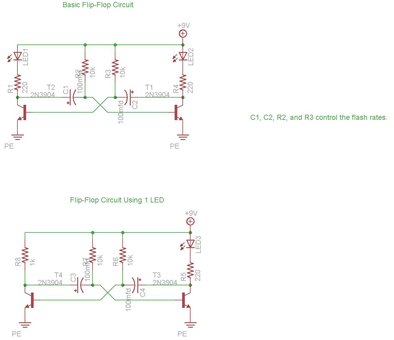 (is there a better page to discuss oscillators?)
Power up low active reset circuit[edit]
Use this circuit with a microcontroller to keep it in reset for a short period of time after the power supply is turned on. Some microcontrollers like this kind of start up. Note that this is really just an application of the RC Filter, also on this page.
ADC Voltage Protection Circuit[edit]
The input to an Analog to Digital Converter (ADC) has some issues that need a bit of attention. The ADC can be damaged by input voltages that are too high or too low. An op-amp is the best way to protect the ADC. (Additionally, an opamp circuit can provide amplification (although this example doesn't); it can remove aliasing noise; and it drives the ADC with low impedance, which can be quite helpful).
This Sallen-Key filter is a specialization of Op amp Non Inverting Amplifier also on this page.
- This opamp circuit is used to
- provide a low input source resistance to the ADC
- protect ADC. Even when the input signal exceeds the supply/reference voltage (i.e. INPUT > Vcc), the voltage into the ADC input pin is capped at the supply voltage.
- Requirement for the op-amp:
- The op-amp can withstand the input signal beyond the supply voltage, provided that the input current is limited to Imax (e.g. OPA4340 Imax = 10mA)
- To reduce noise picked up from the op-amp, use an op-amp with a low Input Voltage Noise Density (measured in nV/√Hz)
- Test conditions:
- Vsignal = 5V
- R1 = 8.2kohm, R2 = 15kohm, C1 = 0.1uF, C2 = 0.22uF
- Measured V+ = 3.8V
- Calculated current = (5-3.8)/23200 = 52uA < 10mA
More Information:
- input protection circuits
- Wikipedia: "Sallen–Key topology"
- Wikipedia: "anti-aliasing" and Wikipedia: "anti-aliasing filter"]
Voltage Divider[edit]
Voltage Divider
We use a voltage divider when we have a voltage that is too big and we just want a fraction ( like 1/3 or .33 ) of it. It is like an amplifier with a gain of less than 1. We use two resistors, the output is always a constant fraction of the input voltage.
Sometimes we use a potentiometer as a voltage divider. This makes the ratio of output to input adjustable. This is how we make a gain control or volume control.
Where
- R1 resistor 1
- R2 resistor 2
- POT a potentiometer
The ratio of input to output is: output/input = R2/( R1 + R2 ).
Discussion
The equation assumes that the input source is low impedance and the output is high impedance, if this is not true consider using a buffer on the input or the output ( Op Amp Unity Gain Buffer or Transistor Emitter Follower ) For audio applications a so called “log taper” pot may be used as it better matches the way in which we hear. If you want a calibrated control you may use a precision “10 turn precision” pot.
More information:
Voltage Divider using a Light Dependent Resistor[edit]
Used to generate a voltage that depends upon light level. With the LDR on the "high side" the voltage will go up when the amount of light goes up. You need to use a resistor in series with the light dependent resistor, this combination lets a variable current flow through the circuit. The voltage across the resistor will vary with the light brightness ( so will the voltage across the LDR, the two will total the input voltage. ) What size resistor should you use? A rule of thumb: Put the LDR in medium brightness and measure its resistance with a ohm meter. Use that value resistor then in medium light you will get 1/2 the input voltage at the output.
Circuit:
Where
- Input = 5v from power supply Vcc
- Output = signal to connect what ever addition circuit
- LDR The Light dependent resistor
- R: A resistor as described above.
Wheatstone Bridge[edit]
Draft Use this circuit when you want to measure the value of a resistor or detect a small change in resistance.
Where
- Input1 Input 1 normally + DC
- Input2 Input 2 normally - DC or ground.
- R1 Resistor 1.
- R2 Resistor 2.
- R3 Resistor 3.
- R4 Resistor 4.
- Output1 Output 1 for null reading.
- Output2 Output 2 for null reading.
- Meter Use to detect meter balance = null = 0 reading.
Discussion:
The circuit is basically two voltage dividers with the output taken across the output of each voltage divider. It is in "balance" when the output is 0. This is true when R1/R2 = R3/R4. The output traditionally went to a galvanometer a very high sensitivity meter. Input traditionally was a battery. By using calibrated resistors for R1, R2, and R3 the value of R4 may easily be calculated. The whole circuit including a wide range of precision resistors, the battery and galvanometer was all packaged in an box and sold as a unit. The same principal can be used with components other than resistors and AC for input instead of DC.
More Information:
- Wheatstone Bridge
- Capacitance Bridge This one is an antique.
current mirror[edit]
(FIXME: fill in details)
Wikipedia: current mirror http://en.wikipedia.org/wiki/Current_mirror
Further Reading[edit]
- FreeCircuitDiagram Lots of circuits, not always so basic, more like projects, but many are quite simple. Some but not elaborate explanation of the circuit.
General Comments[edit]
... do we need another page for not-so-basic circuits such as the Baker clamp ? ... I looked it up and would say it is not so basic. So perhaps Not So Basic Circuits would be a good place to put such things. What do others think? russ_hensel
More not-so-basic circuits: "What are all those parts for??" by R.G. Keen. 2002 shows a "simple" noninverting gain circuit, and explains what all the "extra" parts do.
- Philip C. Todd. "Snubber Circuits: Theory , Design and Application". 1993. [4] has more complex snubber circuits.
- "Choosing components for a triac's snubber" has more complex snubber circuits.
