Difference between revisions of "LCD/Encoder backpack for Fox Board"
(restore cool picture of early prototype) |
|||
| (2 intermediate revisions by one other user not shown) | |||
| Line 57: | Line 57: | ||
== Current state == | == Current state == | ||
| − | * | + | |
| + | * I'm busy writing the firmware. The STK500 and AVR JTAG MkII work well together, in spite of having a bit of a stability problem with the debugWire. | ||
| + | ** debugWire needs a stable clock on the device. It works better now. | ||
| + | * I'm using GCC. It cuts the development time over assembler once your code starts getting more complicated. | ||
| + | * Got the first boards from Olimex. I'll post the schematics and board files (eagle) soon. | ||
| + | * Picture! Yes, I saw the weird component print. I must have botched up the silkscreen fix recommended by Olimex on their site. | ||
| + | |||
| + | [[Image: Lcdui_pcb.jpg]] | ||
| + | |||
| + | Early hand-wired prototype: | ||
[[Image:IMG 7131 (Small).JPG]] | [[Image:IMG 7131 (Small).JPG]] | ||
| − | |||
| − | |||
| − | |||
| − | |||
| − | |||
| − | |||
| − | |||
Latest revision as of 08:09, 8 March 2008
Introduction[edit]
This is a project that I'm working on at the moment, as a learning tool for other projects in the future. The project aims to develop a small board that acts as a backpack for an LCD and a push encoder to provide a UI for a master system. Communications from/to the device would be over TTL level asynchronous serial. The central component is to be an Atmel ATTiny2313.
Goals[edit]
My first target will be the STK500. This will ease development and debugging. I'll hook everything up with those nifty prototyping wires from SparkFun.
Then I'm going to wire it up on a breadboard. I think.
The next targeted master system would be the Fox Board, because I have it readily available. I've been able to get various LC displays working on the Fox Board, but it's pretty clumsy (using these prototyping wires. they're fun, but clumsy). I'm also experimenting with some VFD displays that I was able to obtain. They suck power, but look pretty cool. I will then wire it up using one of their prototyping daughter boards. They are very nice and easy to solder with.
The next target will be a custom board. This board should be mountable behind the LCD with a bit of flexibility. The encoder and the communications would be on a separate header. I'll design it with room for both 16-pin SIL header and 16-pin DIL header for the different types of LCDs that I have. Oh and I want to drive the LCD backlight with a PWM output so that I can "fade" the backlight in and out. I'm keeping the SPI pins available for programming, so you're welcome customize the firmware to use 1-wire, 2-wire or 3-wire interfacing.
Except for the PWM output, the schematic looks like it's compatible with the older AT90S2313. Using surface mount components, you probably wouldn't want to bother trying to find them. If you do, you won't have a PWM output to fade the backlight, but it can still be toggled by driving the pin as a simple digital output.
Motivation[edit]
Everybody and their dog has designed an LCD backpack, it seems. I'm not trying to compete with that.
My motivation for this project is the following:
- Reduce the complexity of supporting an LCD and a push encoder input for a "bigger" master system. Creating kernel drivers to make interrupt based inputs work is such a pain. You don't want to miss one of them quadrature states!
- Learn to design a schematic and a board. When it works, I'll open a bottle to celebrate!
Board Design Notes[edit]
The currently selected use for the ATTiny2313's pins:
- Pin 1: reset/dW: I'll use the debugWire, thankyouverymuch!
- Pin 2: uart rx
- Pin 3: uart tx
- Pin 4: external crystal 3.6864 (necessary for correct UART baudrates)
- Pin 5: external crystal
- Pin 6: int0/pd2 : encoder push
- Pin 7: int1/pd3 : encoder A
- Pin 8: pd4: encoder B
- Pin 9: oc0b: LED backlight PWM
- Pin 10: gnd.
- Pin 11: pd6: LCD enable line.
- Pin 12: pb0: lcd d4
- Pin 13: pb1: lcd d5
- Pin 14: pb2: lcd d6
- Pin 15: pb3: lcd d7
- Pin 16: pb4: lcd command/data
- Pin 17-18-19: ISP for programming can be reused for other communication protocols.
- Pin 20: vcc
Notes on this:
- This is a better setup than the previous one, since it would keep the lcd stuff on the same side (might be easier on the routing).
- I only need 1 interrupt input for the encoder, the other I can read in to read the direction.
- This setup gives me two interrupt vectors, one for the encoder push and the other for the encoder A. This makes programming a bit easier.
- The lcd enable line needs to be toggled, but the command/data bit is written together with the data.
- The downside is that the PWM is not available on the older AT90S2313, so you'll lose "lcd intensity control" on that one. Not that important.
- I wanted to keep the dW and ISP pins free.
- I need the crystal for correct baud rates.
Current state[edit]
- I'm busy writing the firmware. The STK500 and AVR JTAG MkII work well together, in spite of having a bit of a stability problem with the debugWire.
- debugWire needs a stable clock on the device. It works better now.
- I'm using GCC. It cuts the development time over assembler once your code starts getting more complicated.
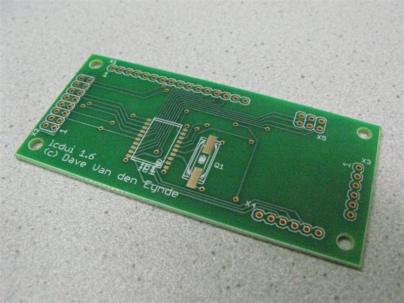
- Got the first boards from Olimex. I'll post the schematics and board files (eagle) soon.
- Picture! Yes, I saw the weird component print. I must have botched up the silkscreen fix recommended by Olimex on their site.
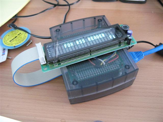
Early hand-wired prototype:

