Difference between revisions of "Programmable Chip EEG"
(→Description of How it Works: convert to active voice) |
|||
| Line 139: | Line 139: | ||
== See also: == | == See also: == | ||
| + | * [http://www.nytimes.com/2008/01/15/science/15robo.html?ex=1359090000&en=69146e0fb3807a74&ei=5124&partner=permalink&exprod=permalink] | ||
* [http://wiki.asiaquake.org/openeeg/published/ The OpenEEG wiki] | * [http://wiki.asiaquake.org/openeeg/published/ The OpenEEG wiki] | ||
* [http://pceegbci.blog.com/ The Open EEG Brain Computer Interface BLog] | * [http://pceegbci.blog.com/ The Open EEG Brain Computer Interface BLog] | ||
Revision as of 05:23, 18 March 2008
Contents
- 1 The Programmable Chip EEG
- 2 PCEEG, What it is and why it can be the best
- 3 News
- 4 Status
- 5 Hardware Overview
- 6 Description of How it Works
- 7 Parts used in the PCEEG:
- 8 ESD Protection in 1168
- 9 A/D Converters
- 10 Electrical Isolation From the PC.
- 11 Software Tools
- 12 Open Source Circuit Design
- 13 ideas for future work
- 14 Open source (public) results!
- 15 See also:
The Programmable Chip EEG
Welcome to the PCEEG Wiki, where everyone can add to this EEG brain-computer interface!
PCEEG, What it is and why it can be the best
- The The Programmable Chip EEG gets its name because its hardware and software can be adjusted digitally from a home pc.
- The Programmable Chip EEG is a Modular Multi-channel electroencephalograph.
- This can be used for a brain-computer interface with biofeedback using a flex sensor or servo to detect fingure movements.
- The LT1168 Programmable-Gain Precision Instrumentation Amplifier is used to amplify the weak electric signals coming from the brain through electrodes attached to the scalp, and has internal protection circuitry for the user.
- Several matched LT1114 Low Power Precision OP-Amps are used for amplification and filtering of the signals.
- ESD Protection in LT1168 Programmable-Gain Precision Instrumentation Amplifier Chips have been chosen that fallow the human body model of esd protection this can be seen in the 1168 datasheet.
- To reduce noise in the readout of the analog part of this circuit, a common-mode feedback is passed back into the body by the driver right leg circuit, for example, 60Hz noise from nearby A/C power wiring.
- The analog signal prossesing board will digitize the signal and pass the data to the control board. The control board is based on the AVR Mega168 which will, further process the signals, and provide an interface to a computer.
- we are using the AVR Mega 168 or Mega8.
- AVR C and the AVR Mega 168 allows for a complete open source system...
News
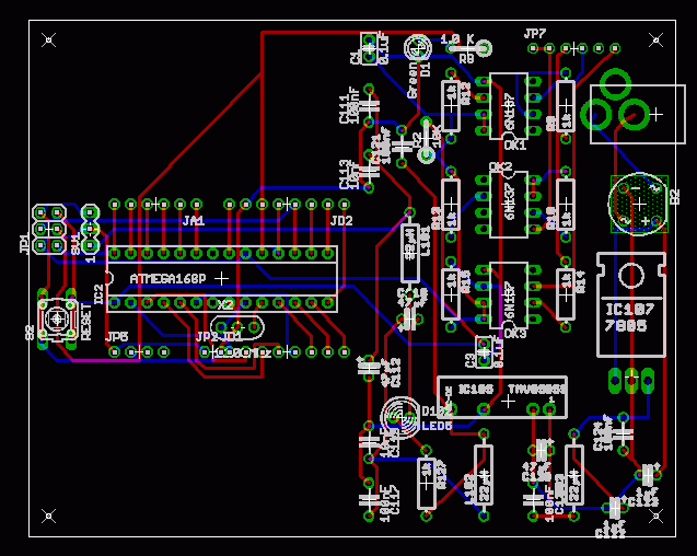
The design is switching from LT switcher CAD (aka LTspice SwitcherCAD) to EAGLE CAD, because the auto-router is excellent for open-source productivity. It will allow the design to evolve faster and with less work with a wider selection of PCB Manufacturers.
The robot arm interface by Miguel Nicolelisis very inspiring. He used implanted electrodes to monitor and allow monkeys to control a robot arm as if it was their own. Could the PCEEG do the same with its electrodes on the scalp. Only the future will show.
Status
- Editing the code of the Open EEG and Monolith EEG to be more portable and utilize avr-libc libraries more.
- Using the open Boarduno design to prototype the design.
Hardware Overview
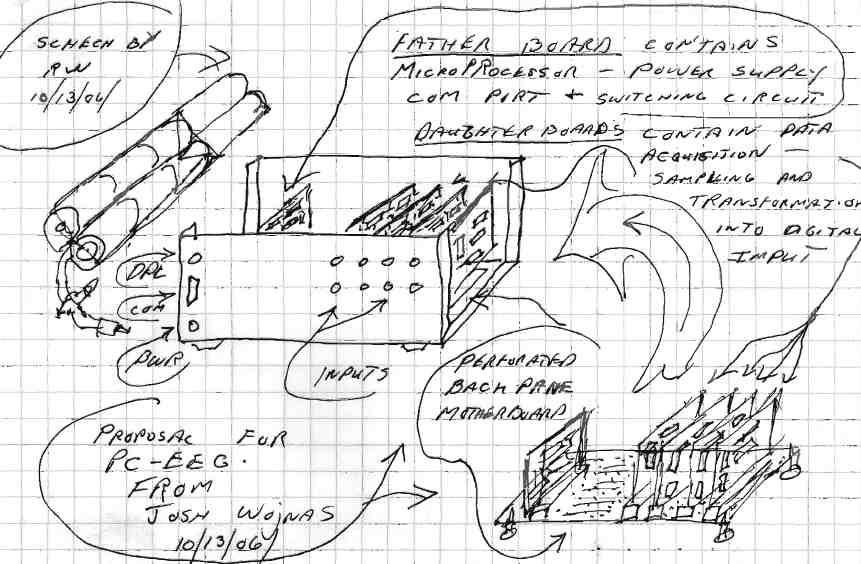
Here is a diagram of how the analog signal processing boards and the microprocessor board will come together.
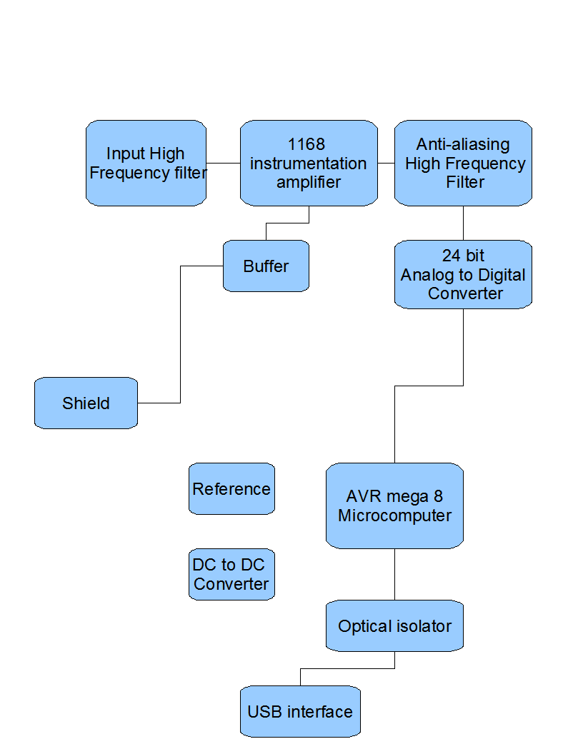
 Here is how the analog signal prossesing board will come together.

Description of How it Works
Neurons in the brain are not perfectly insulated -- some of their electrical activity leaks out and causes (very faint) electrical signals on the skin.
Dry skin is an excellent insulator, so "electrode gel" (typically skin lotion or shampoo) is used to help conduct the electrical signals to the electrode. The researcher tapes the gel-coated electrodes to the skin, or uses a headband to press the electrodes through the hair against the skin. Insulated wires attached to the electrodes bring the signals to the signal processing daughter board.
The signal processing daughter board is responsible for filtering and digitizing the signals from the body. Then the signals are passed to the control board that is the motherboard. The motherboard then can pass the signal to a larger computer.
On the signal processing daughter board is an anti-aliasing filter, an amplifier, and a analog to digital converter. The instrumentation amplifier amplifies the differential analog signal on the input wires. Then the signal is digitized by a a/d converter. The a/d converter has approximately 20 bits accuracy so the signal does not have to be conditioned or filtered as much.
The "right leg driver" circuit on the daughter board is intended to decrease common mode signal. That circuit inverts the common mode signal from the instrumentation amp, sums the result from each instrumentation amp, and sends the total back to the body.
The ADCs simultaneously digitize all the analog signals (really?). The ADCs send bits of information (representing the original analog electrical signals) to the controller motherboard.
The controller board is the mother board of the system. All the signal processing daughter boards plug into the mother board. The controller board is based off the open hardware Boarduino design. The controller board includes a Atmel AVR Mega 168. The controller board can be programmed using AVR GCC.
Working on some other improvements... C123 with 1uF is much too small. Use 1000uF or so instead.

Parts used in the PCEEG:
- LT1168 Resistor-Programmable-Gain Precision Instrumentation Amplifier is used to amplify the weak electric signals coming from the brain through electrodes attached to the scalp, etc.
- Several LT1114 Low Power Precision OP-Amps are used for amplification and filtering of the signal
ESD Protection in 1168
Chips have been chosen that fallow the human body model of esd protection this can be seen in the 1168 datasheet.
To reduce noise in the readout of the analog part of this circuit, a common-mode feedback is passed back into the body by the driver right leg circuit. Band reject filter may also be used (to reject, for example, 60Hz noise from nearby A/C power wiring).
The analog signal prossesing board will digitise the signal and pass the data to the control board. The control board is based on the UBW which will, further process the signals, and provide an interface to a computer & lcd display.
A/D Converters
The programmable chip EEG needs an A/D converter to convert the analog signal (at the output of the instrumentation amplifier) into digital bits. We expect this project to require at least 20 bit ADC. It will amplify the signal less requiring less analog signal processing and use the more sensitive a/d converter to make up for less amplification and cause less signal attenuation.
- $12.00 The ads1255 or ads1256 by ti is a great a2d converter it has programmable gain and digital low pass filtering with 24 bits of resolution 30KSPS. It is a 20-SSOP so it can be soldered by a hotplate or hot air rework tool.
The newest system is a dc amplifier without a high-pass, and all the low-pass filtering is digital
Electrical Isolation From the PC.
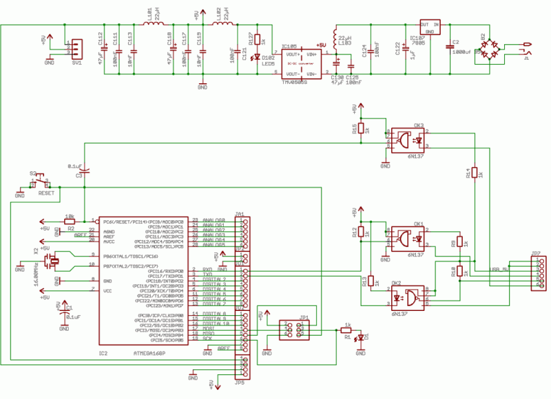
This isolates the PCEEG from the computer when used with a DC to DC converter.
DC to DC converter
The design is based on the modular eeg and monolith eeg they use a TMV0505S, but it is not available in many places. It will be replaced with NMV0505SA. This converter has a rather high output voltage (6-7 V) at very light loads. Therefore, when building the digital board measure the voltage in the +5V/3 of modular eeg designnet, e.g. at IC103 pin 8.
The voltage should be LESS than 6V. If not, you must reduce the value of R127 (near the LED), in order to present the DCDC converter with a higher load.
Optocoupler
A optocoupler by Fairchild 6N137 is used to transfer data from the microprossesor to the Rs232 converter by light.
"The MonolithEEG uses 6N137 opto-couplers which can reliably transmit data at rates above 1MBaud. This provides a simple way to higher sampling rates for the MonolithEEG"
"The ModularEEG allows the replacement of the 6N139 with the faster 6N137. Soley the resistors R125 and R130 on the digital board have to be taken out otherwise both receivers would be disabled permanently."
Software Tools
- EAGLE CAD is being used to create the first PCB. surface mount is used to save space.
- gEDA tools may be a option for opening this design to a wider audience.
- Maxima a computer algebra system s used for graphing and math displays.
- SPI interface code for a/d converters from TI for developers
How You Can Help
- . get the tools
Open Source Circuit Design
- Open Source Circuit Design
- The Programmable Chip EEG Open Source Circuit Design BLog (BrokenLink -- I hope this is only temporarily offline. --DavidCary 10:12, 8 October 2007 (PDT) )
ideas for future work
Currently most EEGs (and EKGs) have "passive electrodes" -- it's a conductive button pressed against the skin, with a long wire that takes the faint signal to the amplifier in the box.
A few EEGs have "active electrodes" -- the amplifier is on top of the conductive button, and sends a strong analog signal down the long wire to the ADC in the box.
User:DavidCary is thinking about going one step further: put the amplifier and the ADC on the electrode, sending out digital packets to the box. Can I do all that with a single chip -- an 8-pin PSoC? Also, instead of each electrode having its own dedicated wire to the data collection box, all the PSoCs are connected in a string (or some other network), forwarding packets from one to the next, so no matter how many electrodes are connected, only about 4 wires (2 power + 2 digital data) are connected. I haven't decided yet whether it's better to have every node do both -- sample data and forward packets -- or if I should split them up, with PSoCs sampling data and sending it to a hub, and hubs (perhaps not PSoCs) forwarding data from a few local PSoCs and from other hubs. --DavidCary 08:50, 10 October 2007 (PDT)
Open source (public) results!
PHP will be used to create a database of users and what they sample and choose to share with the open source community.
The database will give statistical analysis on users recordings.
Also the extension of SETI called BIONIC could be used as a distributed library creation of artifacts and data mining.
Please contribute and make the PCEEG a great tool for researching brain computer interfaces.
See also:
- [1]
- The OpenEEG wiki
- The Open EEG Brain Computer Interface BLog
- EEG Training Seminars
- wiki cities on pceeg
- pceeg.sourceforge.net
- miguel nicolelis
- Maxima - a computer algebra system
- digital high pass filters and other circuits
- human and computer vision lab
- PCB Manufacturers such as www.batchpcb.com
- eeg biofeedback "mind machine"
- monolith eeg
- yet another pundit disrespects the EEG
- lazer cutting for box & solder paste stencil
- Build Your Own Printed Circuit Board
- solder paste for surface mount that can be stored at room temperature
- The thread "amplifying biomedical signals: 150 uA with 16 bit resolution?" has several op-amp suggestions, and mentions that "a good, low-noise, low-cost, isolated EMG/EEG amplifier is one of the most demanding analog electronics designs."
- How to build your own ECG device
- neurofeedback helps musicians improve their musical performances by 13 to 17 per cent.
- "the World's largest Biofeedback and Neurofeedback Discussion Group"
- TI app note "Biophysical Monitoring: Electrocardiogram (ECG) Front End" has a simple circuit: 390 KOhm resistors in-line with each lead -- one end touches patient, the other end directly connected to the instrumentation amp input (or the right-leg drive amplifier output, which has no further protection). The inst. amp has 2 protection diodes on each input, directly to +power and -power. Also, 39 pF capacitor from each input to analog GND, and 200 pF between the 2 inputs. The TI publication "Information for Medical Applications" (2Q 2004) reprints that circuit, but leaves out the caps and the diodes.
- (*) Some people use 420 Hz sampling rate, 10 bits/sample.
- "High-Resolution QRS Detection Algorithm for Sparsely Sampled ECG Recordings" by Timo Bragge et. al. 2004 recommends: "the sampling frequency of the ECG should be at least 500 Hz"
- "Low-Power, Low-Voltage IC Choices for ECG System Requirements" by Jon Firth and Paul Errico says "The multiplexed architecture, based on an old assumption that the converter is by far the most-expensive front-end component, is prevalent in today's electrophysiological measurement systems. However, with the proliferation of sigma-delta converter architectures, converter-per-channel is now a power- and cost-competitive alternative". It also gives a typical schematic for both architectures and suggests some parts.
- Is there a Medical Electronics Forum?
- Make: Homemade Electrocardiograph ([2] recommends skin lotion or shampoo as a low-cost electrode gel)
